What Is PCB Assembly?
PCB assembly refers to the process of assembling all electronic components such as resistors, transistors, diodes, etc. onto a printed circuit board, and the assembly method can be manual or mechanical. People often confuse PCB assembly with PCB manufacturing, they involve completely different processes. As for PCB manufacturing, it involves a very wide range of processes including design and prototyping, whereas printed circuit board assembly begins after PCB fabrication and it’s all about component placement.
3 Types of PCB Assembly Technologies
The progress of electronic technologies has brought more possibilities for PCB assembly. Now there are three commonly used assembly technologies, one is SMT ( Surface Mount Technology), the second one is THT(Thru-Hole Technology), and the third is a combination of the former two.
Surface Mount Technology
SMT Assembly is mainly assembled by soldering surface mount devices (SMD) on the PCB. Since the standard package of SMD components is small, the whole process must be carefully controlled to ensure the high accuracy and the proper temperature of the solder joints. Fortunately, SMT is a fully automated assembly technology that automatically picks up individual components and places them on the PCB with extreme precision.
Thru-Hole Technology
THT is a more traditional PCB assembly technology in which the installer inserts electronic components such as capacitors, coils, and large resistors and inductors into the circuit board through holes. Compared with SMT, through-hole mounting allows the assembly of large-sized components, and it provides a stronger mechanical bond, which is also more suitable for testing and prototyping. more THT PCB Assembly>>
Mixed PCB Assembly Technology
Electronic products tend to be designed to be smaller in size and have more functions, thus placing higher demands on printed circuit board assembly. People need to assemble highly complex circuits in a limited space, it is difficult to achieve the desired effect using only SMD or PTH, we need to combine SMT and THT technology. When using mixed pcb assembly technology, appropriate adjustments must be made to simplify soldering and assembly.
PCB Assembly Process
Step 1: Solder Paste Stenciling
In the first step, solder paste would be applied to the board. The solder paste is grey and consists of tiny metal balls composed of 96.5% tin, 3% silver, and 0.5% copper, be sure to use it in a controlled amount and make sure it is applied in the exact location. In a PCB assembly line, printed circuit boards and solder stencils are held by mechanical clamps and the exact amount of solder paste is applied to the desired areas. The machine will apply the slurry to the stencil until it evenly covers each open area. Finally, when we remove the stencil we can see that the solder paste remains in the correct place.
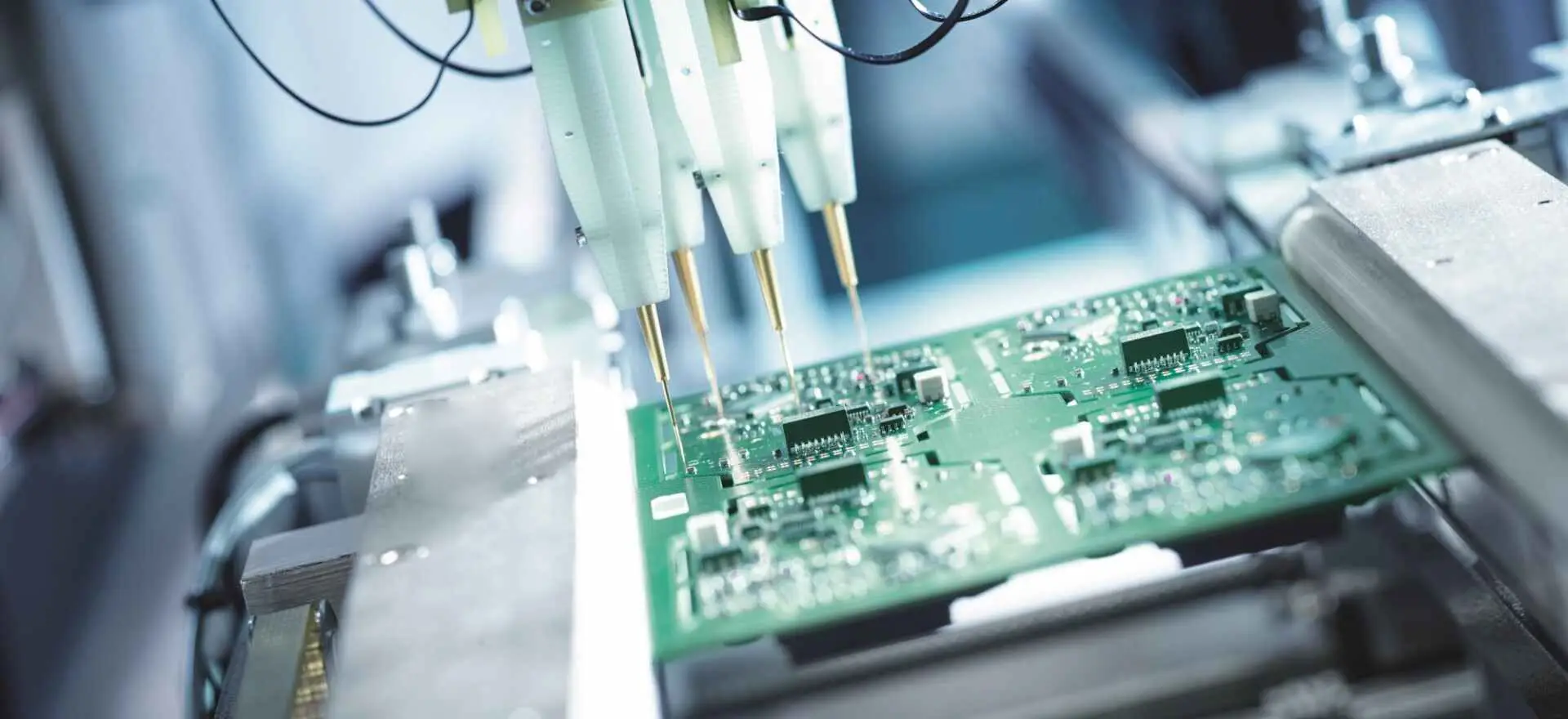
Step 2: Pick and Place
In the second step, we need to use the pick and place machine that can place surface mount components on printed circuit boards automatically. Currently, SMD components are widely used on kinds of PCBs, which can be assembled with high efficiency. In the past, pick and place are applied manually, and the assembler need to pay much attention during the process to make sure that all components are placed in the right position. While the automatic pick and place are operated by robots that can work 24/7 without fatigue, it improved productivity and reduce errors to a large extent. The machine picks up printed circuit boards with its vacuum grip and then moves them to the pick and place station. The robot then positions the PCB on the station, and the SMD components would be placed on top of the soldering paste in intention locations.
Step 3: Reflow Soldering
After the pick and place, the PCB assembly would move to the reflow soldering process. The circuit boards would be transferred to a large reflow oven through the conveyor belt. The oven would heat the boars at high temperatures, normally about 250 degrees Celsius, to melt the solder in the solder paste. When the heat process is finished, the circuit boars would be moved through the oven which consists of a series of cooler heaters, which would help to cool and solidify the melted solder. During the reflow soldering, we should pay attention to some special boards, taking two-sided PCBs for instance. Each side of two-sided PCBs needs to be stenciled and reflow soldered separately, normally, the side with fewer components would be reflow soldered first, then the other side.
Step 4: Inspection
The assembled circuit boards need to be tested for functionality the reflow process may result in poor connection or even lack of connection. The movement during the reflow soldering may also cause the shorts. Thus, inspection is a key step involved during the assembly process. There are a variety of methods to inspect errors, and the commonly used ones are manual checks, x-ray inspection, and automatic optical inspection. Periodic inspections can be performed after reflow soldering, so any potential problems can be identified until the circuit card assembly moves on to the next process. Such inspection can help manufacturers save a lot of money because the sooner they detect a problem, the sooner it can be resolved without wasting time, human resources, and materials.
Step 5: Through-Hole Component Insertion
Apart from SMD components, some circuit boards may need to be assembled with other kinds of components like through-hole or PTH components. So how to assemble these components? Well, there are plated holes in the circuit boards, which provide access for PCB components to transfer signals from one side to the other side of the board. Thus, soldering paste is workable in this case, so we need to use other soldering methods to insert PTH components such as manual soldering and wave soldering.
Step 6: Functional Test
In the last step, the final inspection will be performed to test the functionality of PCBA, we call this process a “functional test”. This test will simulate the normal operation of the PCB, and monitor the electrical characteristics of the PCB when the power supply and analog signal pass through the PCB to judge whether the PCBA is qualified.
Suggestions to Perform PCB Assembly Better
After explaining the detailed process of printed circuit assembly, now we would like to offer some suggestions that can improve the quality of the PCBA.
- Component size
It is of great importance to select the correct package size for each component on the boards during the PCB design period, generally speaking, we suggest choosing larger packages. Choosing smaller packages may result in potential problems during the circuit card assembly phase, which would take a lot of time to modify the circuit. While for some complicated modification such as disassembling and soldering components, assembling the whole circuit board again is much easier.
- Component footprint
The component footprint is another key consideration of PCB assembly. Each footprint must be created precisely according to the land pattern specified in each integrated component’s datasheet. Many problems can arise from an incorrect footprint, such as causing uneven heat applied to the integrated component during the soldering process, causing it to stick to only one side of the PCB instead of both sides. In addition, passive SMD components such as resistors, capacitors, and inductors would also be affected mainly due to incorrect dimensions of the land pattern associated with the component, and different magnitude of the tracks connected to the two pads of the component, or the track width being too wide.
- Spacing between components
Overheating caused by insufficient space between components is one of the main causes of PCB failure, and this problem is more pronounced in some highly complex circuits. Placing one component too close to another can cause a variety of problems, the most serious of which can lead to redesign and re-fabrication of the PCB, which is a time-consuming process that adds unnecessary costs. When we apply automated assembly and test machines, it is important to ensure that each component is kept a far distance from mechanical parts, the edge of the board, and all other components. Too little spacing between components or components that are rotated incorrectly can cause problems during the wave soldering process. For example, if a higher component precedes a component with a lower height along the path traveled by the wave, the weld will weaken.
- Updated BOM
For both PCB design and assembly processes, it is vital to make sure that the bill of materials(BOM) is always updated. Any mistakes or inaccuracies of BOM can bring big troubles, which may postpone the whole assembly phase as manufacturers need to spend much time to figure out and solve the problem. To make sure the accuracy and validity of BOM, every time you update your PCB design, you should review the BOM thoroughly and carefully. For instance, if there is a new component is added to an existing project, then it is necessary to make sure the BOM is updated accordingly.
- Use of fiducials
Fiducials are rounded copper shapes, they would play the role of landmarks for pick and place assembly machines. By using fiducials, automated equipment can identify board orientation and assemble fine pitch surface mount components. Fiducials can be divided into two classes that are global fiducials and local fiducials. Global fiducials are used to place on the edge of the printed circuit boards so that the orientation of the board in the X-Y plane can be detected by pick and place machines. As to Local fiducials, they are placed close to the corners of square SMD components, which allows pick and place machines to locate the footprint of a component accurately that can help reduce the positioning errors during PCB assembly. In a word, fiducials are very important for PCB assembly, especially when there are many components involved on the board that are not far from each other.
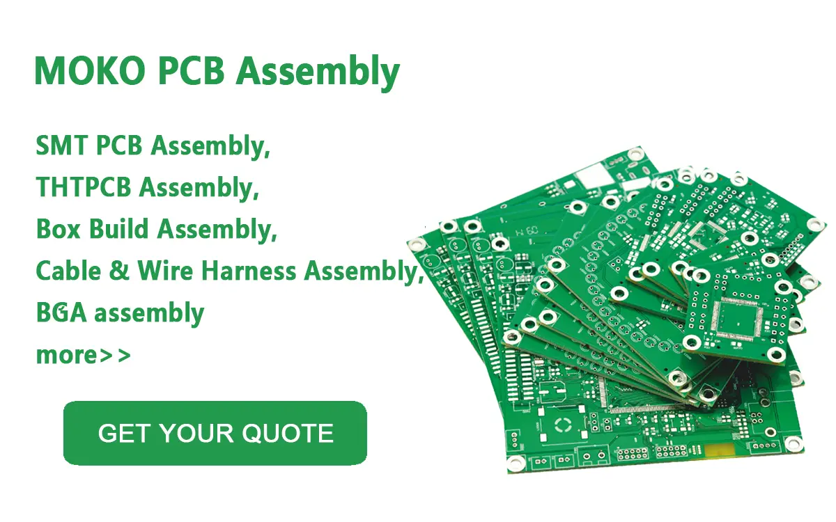
PCB Assembly Service at MOKO
MOKO Technology is a leading PCBA provider in China, certificated with ISO9001, ISO14001, ISO13485, IPC, and UL. We are committed to providing high-quality PCB assembly service by leveraging our 16 years of experience and expertise, which make us confident to meet kinds of assembly requirements well.
Almost everything can be assembled here, we provide a full-coverage PCB Assembly service including SMT, THT, Box Build, Wire Harness, and BGA assembly. Our engineers are experts in
printed circuit assembly who would work with you closely and offer suggestions to make sure the feasibility of your assembly projects. From prototype assembly boards, low- to high-volume circuit boards, and everything in between, we can always provide superior PCBA to our customers with a short turnaround time.