Prima dei circuiti stampati (PCB) e i PCB assemblati lasciano la fabbrica, vengono sottoposti a test rigorosi per individuare eventuali problemi con i circuiti o le connessioni elettriche. Questi test aiutano a garantire che le schede siano affidabili e funzionino bene nei prodotti finali. E molti produttori di PCB utilizzano un approccio di test prevalente chiamato test della sonda volante. In questo articolo, I’ll explain what flying probe testing is, how the process works, and other commonly used testing method for PCB and PCBA. To start, let’s look at what exactly happens during a flying probe test.
What Is PCB Flying Probe Test?
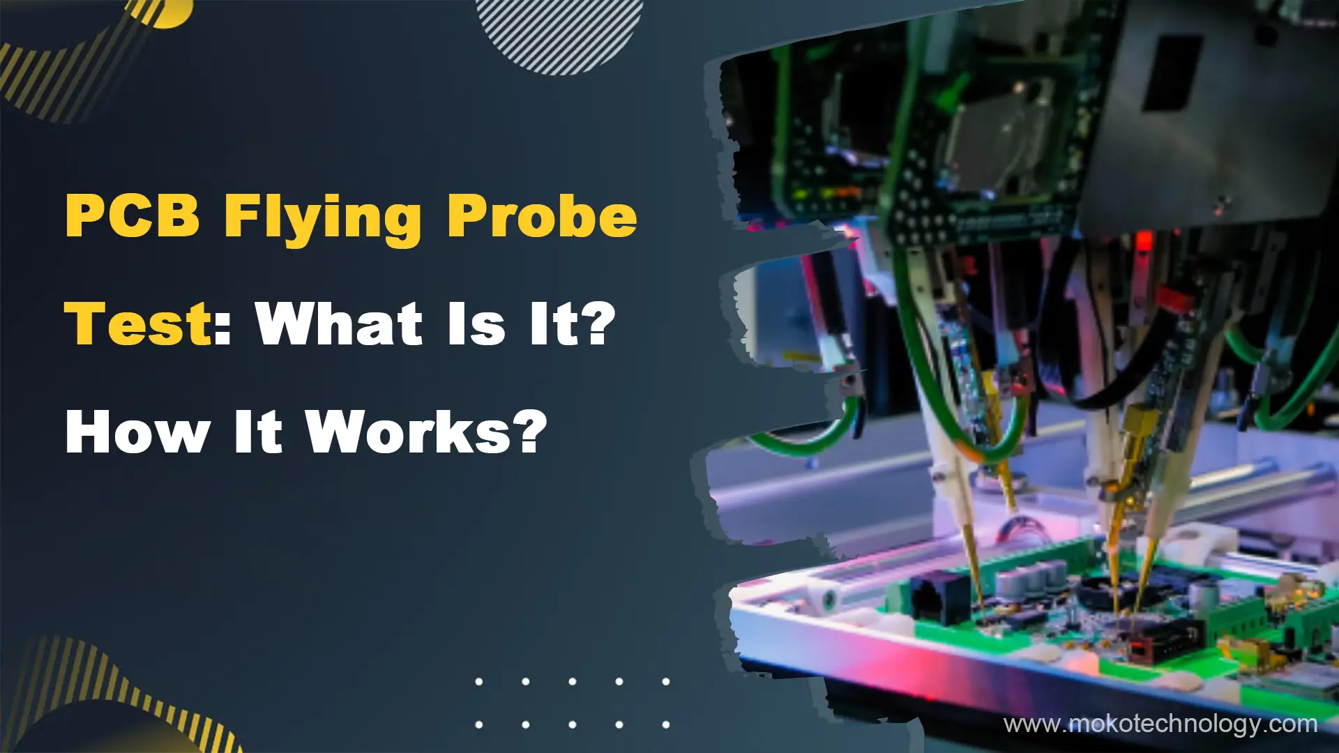
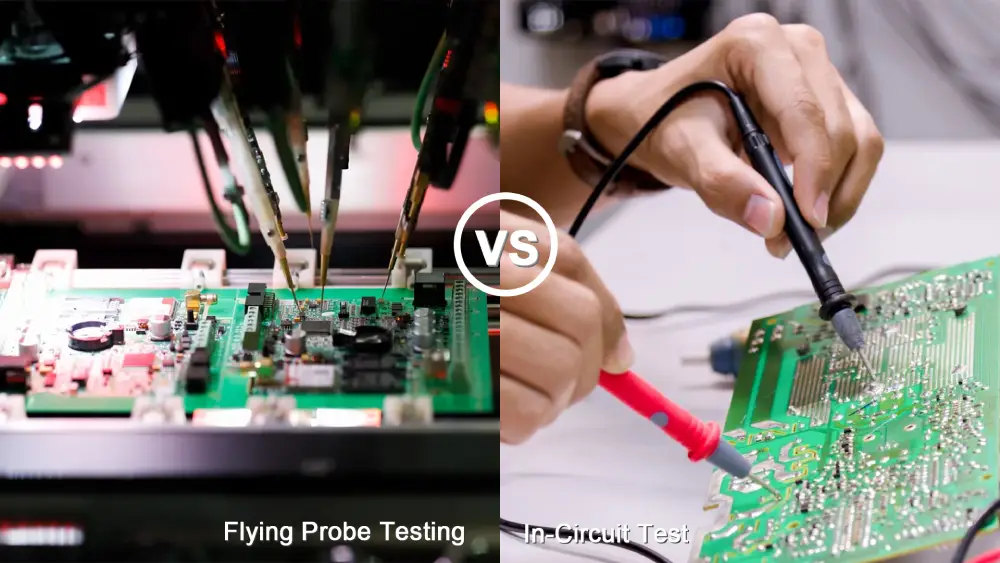
Flying probe testing uses movable probes that can make contact at multiple test points on the board simultaneously. This method utilizes probes that can move around and “fly” to different locations on the circuit board. The probes contact both the top and bottom of the board to reach test points. They are able to travel to test various conductors or components, and then move to another area of the board to test something else. Since the probes are not limited in their access to the board and can test countless connection points, flying probe testing offers a cost-efficient solution for boards in the early development stages. It performs non-powered checks for capacitance, diode function, inductance, si apre, resistenza, pantaloncini, e altro ancora.
How Does Flying Probe Testing Work?
- The testing engineer takes the CADdata for the PCB that needs to be tested. This data is input into the test program, which enables the testing unit to map out the layout of the PCB and PCB componenti. And the data is combined with specifications for the board to identify which areas need testing.
- The unit under test (UUT) is placed on the tester via a conveyor belt.The probes are coded to move along the X-Y axis of the board, traveling from point to point. This allows the headers to contact each test point individually.
- As the probe makes contact, it runs an electrical current through each connection.The current flows back through a multiplexing system and sensors, which measure the signal. Components not being tested are shielded to avoid signal disturbance. The readings detect any shorts or faulty components. A camera provides close-up viewing of the UUT to identify physical issues.
Vantaggi e Limitations of Flying Probe Testing
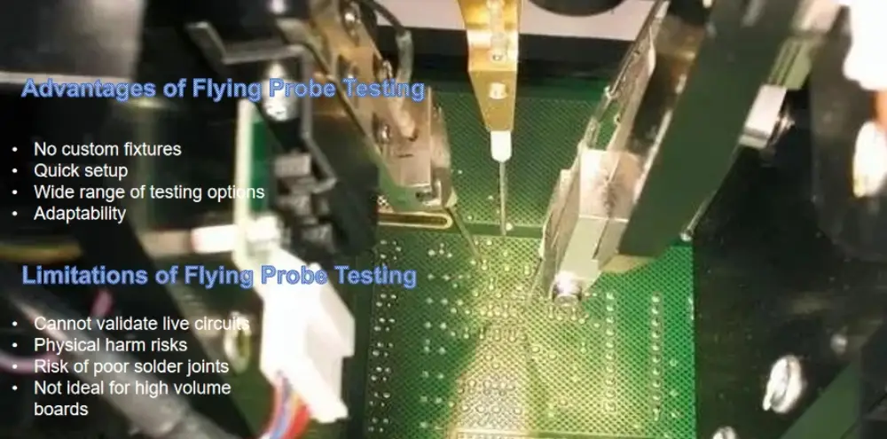
Advantages of Flying Probe Testing
- No custom fixtures
Flying probe testing eliminates the need for expensive, time-consuming custom fixtures. The probes can be programmed to target any test point on the board without fixtures. This flexibility saves time and cost compared to bed-of-nails testing which requires designing and fabricating custom fixtures. For low-volume or prototype boards, a flying probe is an ideal fixtureless testing solution.
- Quick setup
One of the major benefits of flying probe testing is the ability to set up the testing process in a relatively short timeframe. It leverages programmable flying probes that can be quickly configured to make contact with test points on a printed circuit board.
- Wide range of testing options
Flying probes can perform a full array of test types during a single pass, including continuity, resistenza, capacità, voltaggio, e test funzionali.
- Adaptability
If the board design changes, the flying probes can be quickly reprogrammed to the new layout without having to modify tooling. This reduces costs and delays.
Limitations of Flying Probe Testing
- Inability to validate live circuits
Flying probe testing does not power up the circuit during the test. This prevents validation of the fully functioning product. The unpowered nature provides only partial testing.
- Potential physical harm
Direct contact from the probes can dent or damage the via and pad surfaces on the board. Some manufacturers see these small dents as defects, though improving probe technology may resolve this.
- Risk of poor solder joints
Probes sometimes touch component leads rather than landing on test pads. This contact can potentially loosen or weaken solder connections.
- Not ideal for high volume complex boards
The limited number of probes must cover all test points across large, complesso, high volume boards. This extensive required coverage becomes problematic and inefficient compared to solutions like fixture testing.
Flying Probe Testing vs. Test in-circuit (ICT)
When testing completed printed circuit board assemblies, manufacturers must choose between two prominent methodologies: test delle sonde volanti (FPT) and in-circuit testing (ICT). Both approaches aim to verify overall board functionality and identify any PCB assembly issues or component faults, but utilize different techniques and equipment to perform testing.
What Is In-Circuit Testing (ICT)?
Test in circuito, or ICT, is a method that relies on customized fixtures to test assembled printed circuit boards. These fixtures include probes meticulously positioned to establish electrical connections with the test points on the board undergoing assessment. The fixtures provide access to critical parts of the circuit so test signals can be injected and measurements taken to validate the assembly. ICT systems check for common PCB assembly defects like open or short circuits, missing or wrongly inserted components, and improper resistor/capacitor values. By designing fixtures specifically tailored to a Progettazione PCB, all key components and circuit nodes can be efficiently tested at once for complete test coverage.
Differences between Flying Probe Testing and In-Circuit Test
While ICT testing relies on large racks of complex dedicated fixtures, flying probe testing takes a more flexible approach by using probes that can move across the board and contact points of interest. Rather than developing custom tooling, FPT systems depend on programming developed from CAD data that guides the probes to target locations on each board dynamically. Though both methods involve testing via probes, FPT and ICT differ significantly in practical application:
- Efficacia dei costi
FPT avoids expensive fixturing costs by programming for any layout based on available CAD data.
Runs of prototype or low volume boards can be tested without investment in custom fixtures. però, very high volume production runs with unchanging designs may justify the fixture expense of ICT.
- Accessibility
The large fixed pins of an ICT fixture must be custom-designed for each board and can face physical access limitations. In contrasto, flying probe test uses miniature movable probes that can reach almost any location on the board without issues.
- Flessibilità
When switching between different PCB designs, ICT testing engineers must undergo lengthy changeover procedures to reconfigure pin mappings. però, flying probe test systems can quickly adapt testing via software for various boards. This makes FPT better suited for high-mix, low-volume production.
- Test Coverage
ICT tests leverage a parallel “bed of nails” to access many points simultaneously and completely verify powered performance. While flying probe test probes are nimble, the sequential nature of testing can miss certain defect types. Functional flaws are also harder to detect without power applied during FPT.
Other Commonly Used PCB Testing Methods
In addition to flying probe testing and in-circuit testing, printed circuit boards must undergo a variety of other tests to fully validate performance and quality. Some other commonly used PCB testing techniques include:
- Test funzionale
Functional testing is performed to verify that the printed circuit board is working properly and all the circuits, componenti, and interfaces are functioning as designed. Tipicamente, this process involves linking the circuit board to a test fixture and subsequently evaluating the board’s functionality.
- Ispezione visuale
It is the most fundamental test used by PCB manufacturers. It simply involves looking over the completed board carefully to check for any noticeable flaws or defects. During visual inspection, technicians will scan all areas of the board looking for issues like poor solder joints, incorrect component placement, damaged traces, board contamination, e altro ancora.
- Ispezione a raggi X.
One of the more advanced testing methods used for printed circuit boards is Ispezione a raggi X.
This allows manufacturers to look inside the board and identify any hidden issues that can’t be detected through basic visual examination.
- EMI Test
Printed circuit boards are often subjected to electromagnetic interference (EMI) analisi. This assesses how well the board can withstand and operate normally in environments with electromagnetic noise and interference.
- Electrical Test
One essential set of tests for printed circuit boards focuses on validating the key electrical characteristics of the board itself. Prove elettriche includes checks for resistance, inductance, and capacitance.
