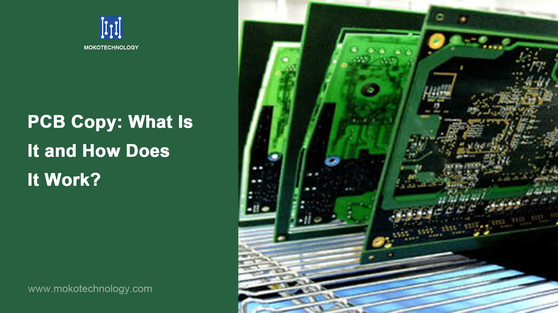
PCB copy has become increasingly popular in recent years as it enables manufacturers to copy existing PCB designs, składniki, itp. to create a new identical circuit board. And there is no need to design the circuit board from scratch, w związku z tym, PCB cloning can save a lot of costs and time by shortening the manufacturing process. W tym artykule, we will explain how to copy a PCB step by step, zanurkujmy prosto w.
What Is PCB Copy?
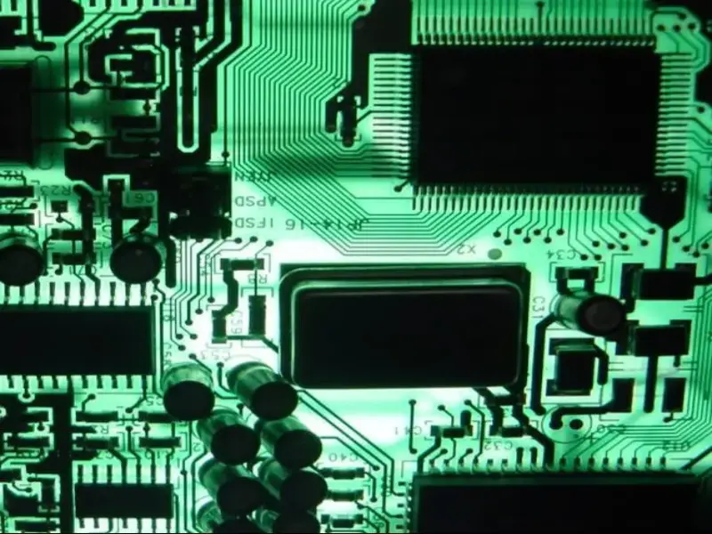
Kopia PCB, also known as PCB cloning, is a process that allows manufacturers to create an exact replica of an existing PCB design. By using this technology, companies can leverage reverse engineering techniques to analyze and recreate the features, specyfikacje, and layout of a particular circuit board. This process involves using specialized software, hardware tools, and expert knowledge to deconstruct the original board and reproduce an identical copy.
Benefits of PCB Cloning
Sumienna inżynieria: Reverse engineering forces engineers to perform an in-depth analysis of the product, leading to top-tier quality designs. It ensures fail-safe and reliable products aligned with customers’ wymagania, improving chances of success.
Stała i doskonała wydajność: PCB copy ensures all boards have the same design and materials, delivering consistent performance with minimal variance, even in mass production. Reverse engineering guarantees extreme care and attention to detail, resulting in superior performance.
Economical and Cost-Effective: PCB copy reduces costs associated with design, prototypowanie, testowanie, and optimization. With an existing design that meets customer needs, manufacturers can perform better quality control and assurance, making the process more cost-effective and practical.
Improved Degree of Freedom and Scalability: PCB copy allows manufacturers flexibility in production operations and customization. It enables scalability, producing large quantities of identical PCBs to meet customer demands and generate more revenue. Manufacturers can align with clients’ supply chains and deliver orders faster.
Streamlined Production: By combining successful PCB designs, manufacturers can automate processes, reducing manual labor costs and ensuring durable, high-performance boards. Streamlining enables handling bulk orders while improving product quality.
How to Copy a PCB: Step-by-Step Instructions
Krok 1: Understand the original PCB design
Before starting the cloning process, it is crucial to understand the electrical parameters and requirements of the original PCB design. You need to get the DOBRZE(Zestawienie materiałów) and the schematic diagram first, as it shows how each component is electrically connected to others. Następnie, review the schematic carefully to comprehend the voltage, aktualny, power requirements, and the interconnection of each component.
Krok 2: Determine components and layout
Capture high-resolution images of each layer of the original PCB, meticulously documenting the specifications, layout and direction of every components, such as diodes, tranzystory, and IC chips. This allows for better layout replication.
Krok 3: Get the board ready for scanning
Carefully remove all surface-mounted components and mechanical connections from the circuit board. Use alcohol to clean the circuit board surface to ensure a clearer scan. Then place the bare board into the scanner and adjust the scanner settings to capture a clear image.
Krok 4: Scan the top & bottom layers of the PCB
- Use color scanning to scan the circuit board and record all symbols, branding, text and identifiers. Następnie, save the image and print it.
- Polish the top and bottom layers of the board to ensure the copper film is clearly visible.
- Rescan both layers separately, making sure the plate is positioned appropriately in the scanner to ensure accuracy.
- Adjust the contrast and brightness in the image to clearly distinguish the copper and copper-free parts. Convert the image to black and white to evaluate whether the lines appear clearly.
- Save the images in black and white BMP format and name them TOP.BMP and BOT.BMP.
Krok 5: Create a New Design File
- Use PCB design software to convert the TOP.BMP and BOT.BMP files to the PCB file format (such as Gerber or CAD).
- Import the converted file into a PCB editor and generate two separate layers – top and bottom.
- On the top layer, lay out the circuit traces and position components according to the scanned TOP.BMP image. Make sure the silkscreenlayer is imported correctly.
- On the bottom layer, trace the necessary lines based on the scanned BOT.BMP image, treating it as a silk screen layer. Once done, remove the silk screen layer from both layers.
- In the CAD environment, using the PCB image as a reference, copy and arrange the component footprint with accuratepodkładka lutownicza
- Carefully check if the pad and via locations on both layers are accurate.
- Wreszcie, import the top and bottom layer files into PCB design software and combine them into an integrated design drawing.
Krok 6: Validate the new design
- Use a laser printer to print out 1:1 transparency film according to the new design file.
- Carefully lay these clear films onto the original PCB for visual comparison.
- Thoroughly review the design to verify accuracy of components, znajomości, rozstaw, rozgromienie, and clearance requirements.
- After verification, continue the manufacturing process using the cloned design.
Krok 7: Test the Cloned PCB
Once fabrication is complete, you need to test the cloned PCB to ensure it functions the same as the original design.
Is It Legal to Copy a PCB?
The legality of copying a PCB design depends on intellectual property rights and the terms on which the original design was obtained. Cloning is generally allowed if you legally purchased or acquired a PCB design with clear rights to modify and copy, such as open source hardware or a public domain design. jednak, unauthorized copying of a copyrighted or patented PCB design to which you do not own the legal rights may constitute intellectual property infringement. Certain limited exceptions may apply, such as copying for personal use, Badania, naprawic, or reverse engineering for interoperability purposes, but these exceptions vary by jurisdiction and have specific limitations.
Końcowe przemyślenia
PCB copy brings a lot of convenience to manufacturers, helping them speed up the production process and reduce costs. But you must make sure everything is done within the limits of the law. MOKO Technology complies with laws and regulations, we provide partners with high-end PCB copy services for many years. Skontaktuj się z nami for a free consultation on related services.