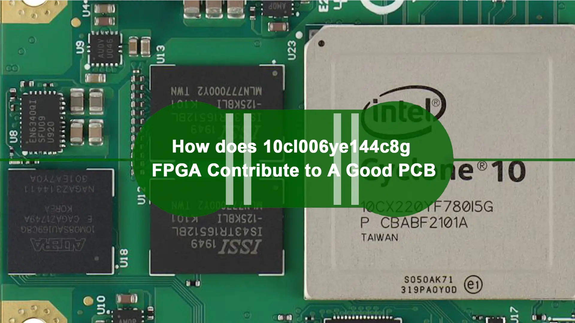
Elektronik cihazlar hızla gelişiyor, kompakt tasarımlar ve verimlilik gerektirirler. Önemli olan birçok seçenek arasında, QFN paketleri tüm zamanların popüler tercihidir. Bu tür paketleri bu kadar popüler yapan şey nedir?? Projelerinizde de kullanmalısınız? Bu kılavuz konuya net ve kapsamlı bir bakış sunuyor.
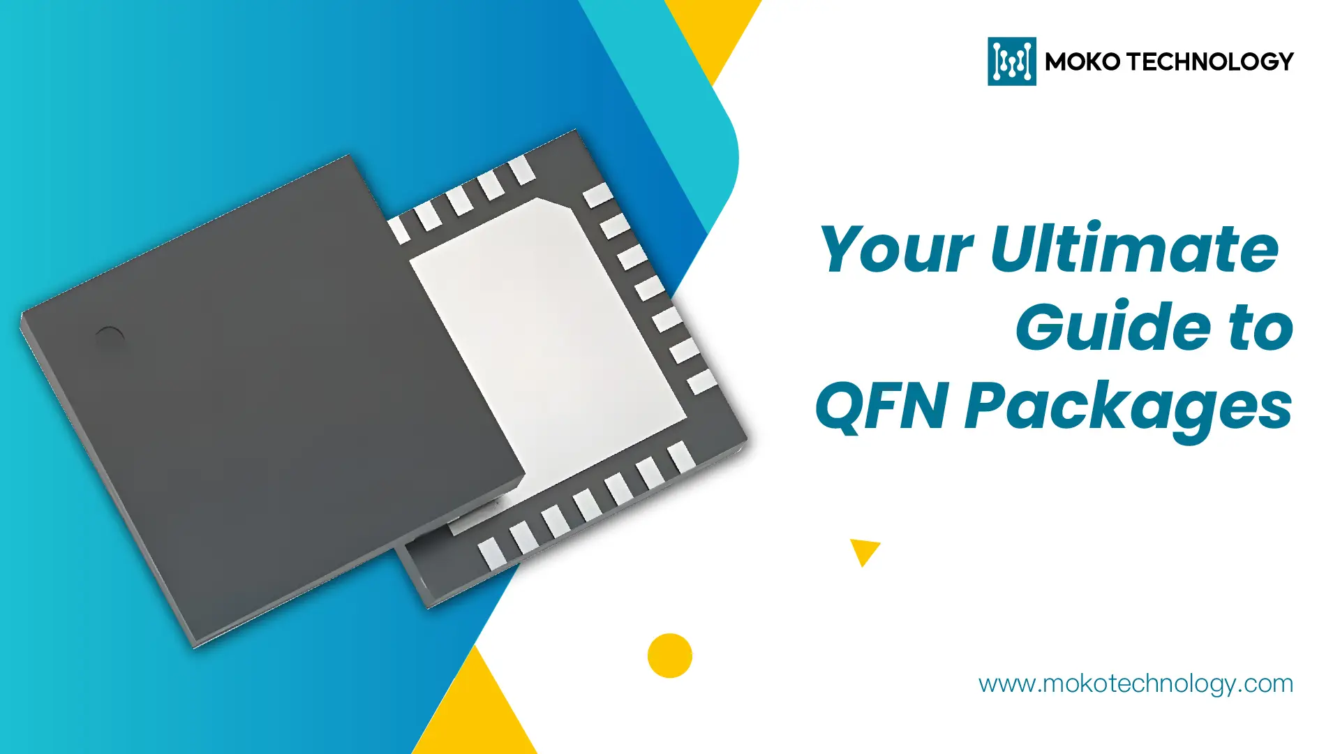
QFN Paketleri Nelerdir??
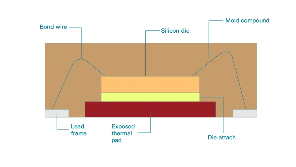
QFN, Quad Flat No-leads anlamına gelir. QFN paketleri silikon kalıpları bağlar (ASIC) baskılı devre kartına (PCB). Kullanılarak uygulanır Yüzey Montaj Teknolojisi. Adından da anlaşılacağı gibi, bu paket geçmişte mevcut olan klasik potansiyel müşterileri içermiyordu. Her zamanki potansiyel müşterilere sahip olmak yerine, Dörtlü düz kurşunsuz paketlerde açık kenar pedleri bulunur lehim pedi altında. Bu yapı elektriksel ve termal performansı artırabilir, QFN paketlerinin kullanıcılar arasında çok popüler olmasının nedeni budur.
Bir QFN paketi genellikle aşağıdaki temel bileşenlerden oluşur:
Kurşun Çerçeve: Bu kısım IC performansının belirlenmesinde çok kritiktir.. Temel olarak paket için destek görevi görür.
Tek veya Çoklu Kalıplar: Bunlar aslında paketin içindeki silikon çiplerdir ve yüzeye montaj tekniği kullanılarak devre kartına monte edilirler..
Tel Bağlar: Bunlar genellikle bakır veya altından yapılır. Bu teller kurşun çerçeve ile kalıplar arasında gerekli bağlantıları oluşturur.
Kalıplama Bileşiği: Bu malzeme dahili bileşenleri çevreler ve korur. Elektrik yalıtımı sağlar, korozyonu önler, ve paketin dayanıklılığını ve güvenilirliğini güçlendirir.
Dörtlü Daire Kurşunsuz Paket Çeşitleri
- Hava boşluğu QFN: Bu tip plastik veya seramik bir kapakla karakterize edilir, bakır kurşun çerçeve, ve plastikten kalıplanmış, mühürlenmemiş bir gövde. Bu tip genellikle arasında çalışan mikrodalga sistemlerinde kullanılır. 20 için 25 GHz, hava boşluğunun gerekli olduğu yerlerde
- Çok Sıralı QFN Paketi: Bu tip tasarım, birden fazla pin sırası kullanılarak yüksek sayıda pinin gereksinimlerini karşılar, benzer BGA teknolojisi ancak çoğu zaman daha düşük bir fiyata yapılır.
- Islanabilir Yanlara sahip QFN: Bu tip dörtlü düz kurşunsuz paket, paket gövdesinin dört tarafında da açıkta metal yanlara veya terminallere sahiptir. Tüm bu kenarlar lehimle ıslanabilecek şekilde tasarlanmıştır ve bu şekilde, Lehim, paket ile PCB arasında fitillenme ve güçlü bir lehim bağlantısı kurma olanağına sahip olacaktır..
- Fc-QFN Paketi (Flip-Chip Dörtlü Düz Kurşunsuz): Bakır kurşun çerçevede flip chip bağlantılarını kullanır. Ayrıca normal bir QFP paketinden daha küçüktür ve elektrik yolunun daha kısa olması nedeniyle elektrik performansını da daha iyi hale getirir.
- Tel bağı QFN: Tel bağ QFN paketinde, yarı iletken kalıp bir kurşun çerçeve üzerine monte edilir ve, daha sonrasında, paket terminallerini yarı iletken kalıba bağlamak için tel bağlar kullanılır. Bu, elbette, normalin aksine daha küçük bir paket ayak izi bırakır Dörtlü Daire Paketleri (QFP'ler) açıkta kalan uçlarla.
Delme Tipi QFN ve Kesilmiş Tip QFN karşılaştırması
QFN paketleri ayrıca üretim sürecine bağlı olarak iki ana türe ayrılabilir.:
Delme tipi QFN: Bu tarz tek kalıp boşluğu ile üretilmektedir.. Kalıplama işleminden sonra her bir paketi kalıplanmış matristen çıkarmak için özel bir alet kullanılır. Bu yöntem seri üretim için çok verimlidir ve genellikle temiz bir sonuç verir., keskin kesim.
Kesilmiş tip QFN: Diğer yandan, testere tipi QFN'ler kalıp dizisi işlemiyle üretilir. Bu, bir testere kullanılarak ayrı birimler halinde kesilen büyük bir kalıplanmış paket tabakasının yapılması sürecini içerir.. Teknoloji büyük hacimlerin yönetilmesinde oldukça etkilidir.
QFN Paketlerinin Avantajları ve Sınırlamaları
Avantajlar:
- Kompakt ve düşük profile sahip olduğundan akıllı telefonlar gibi cihazlarda yer kısıtlaması olan uygulamalar için idealdir, giyilebilir ürünler, ve IoT cihazları.
- Termalin PCB'ye daha verimli bir şekilde aktarılmasını sağlayan açık kalıp pedi sayesinde daha iyi termal dağılım.
- Daha yüksek termal verimlilik, daha iyi performans ve güvenilirliğe dönüşür.
- Boyut olduğunda uygulamalar için iyi, ağırlık, ve güç tüketimi çok kritik faktörlerdir.
Sınırlamalar:
- Hiçbir harici kablo, lehim bağlantılarının görsel incelemesini veya yeniden işlenmesini kolaylaştırmaz, paketin gövdesinin altında gizli olan.
- Küçük pin aralığı ve daha yüksek sayıda G/Ç için, daha yüksek bir risk var lehim köprüleme, ve bunlardan kaçınmak için süreçlerin çok iyi kontrol edilmesi gerekiyor.
- Bazı yüksek güvenilirlik amaçları için pek ideal değil.
QFP vs. QFN: Fark ne? Aralarında Nasıl Seçim Yapılır??
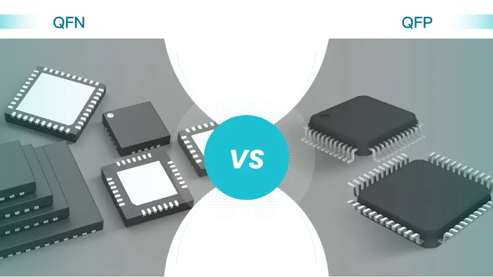
QFP ve QFN en yaygın iki entegre devre paketidir. İsimleri yalnızca bir harf farklı olsa da, QFP paketi, paket gövdesinden çıkıntı yapan martı kanadı uçlarına sahiptir. Bu, incelerken veya yeniden çalışırken çok faydalıdır., ve aynı zamanda, oldukça kompakt.
Kalıp yastığı açıkta olduğundan QFN'ler daha iyi termal yayılıma sahip olacaktır, ve bu tip tasarım PCB'ye daha fazla ısının aktarılmasını sağlar. ancak, Lehim bağlantılarının paketin altına gömüleceğinden dolayı QFN'lerin görsel olarak incelenmesi ve yeniden işlenmesi zordur..
Bileşen için panodaki alanı göz önünde bulundurun, termal performans ihtiyacı, ve üretim sürecinin yetenekleri. İhtiyaç alan ve termal performans ise, o zaman QFN'ler seçim olabilir, ancak ihtiyaç duyulan şey denetim kolaylığı ve yeniden işleme kolaylığı ise, o zaman QFP'ler daha iyi bir alternatif olabilir.
daha fazla okuma: IC Paket Türleri: Doğru Olanı Nasıl Seçersiniz??
QFN Paketlerinin Uygulamaları
QFN paketleri özellikle yerden tasarruf etmenin ve üstün performansa sahip olmanın büyük önem taşıdığı sektörlerde popülerdir. QFN'ler aşağıdaki sektörlerde kullanılmaktadır:
- Tüketici elektroniği: Dörtlü düz kurşunsuz paket, az yer kaplama ve mükemmel ısı yönetimine sahip olma genel amaçlarıyla akıllı telefonlarda ve tablet PC'lerde yaygın olarak kullanılır..
- Otomotiv Sistemleri: QFN paketlerinin yüksek performansı, onu motor kontrol üniteleri gibi hayati modüllerde kullanılan bir cihaz haline getirir.
- Haberleşme Aparatı: QFN'ler, hızlı sinyal işlemenin gerekli olduğu yüksek hızlı ağ cihazlarında uygulama bulur.