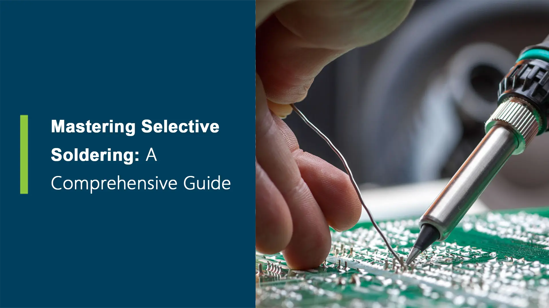
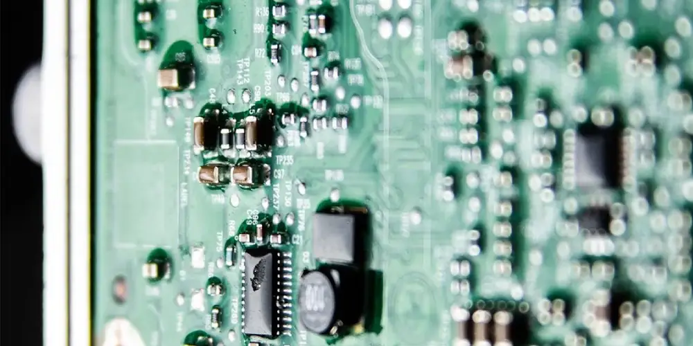
PCB są szeroko stosowane w różnych gospodarstwach domowych, przemysłowy, wojskowy, i sprzęt motoryzacyjny. W celu zapewnienia działania sprzętu i przedłużenia żywotności, ważne jest, aby upewnić się, że płytki drukowane i elementy na płycie są chronione przed wszelkimi zagrożeniami, gdyż każdy błąd w nich może wpłynąć na wydajność urządzenia, a nawet spowodować awarię całego urządzenia. Powłoka PCB jest bardzo skutecznym sposobem ochrony PCB.
W tym ostatecznym przewodniku, omówimy wszystko, co musisz wiedzieć o powłokach PCB 2023 – od rodzajów materiałów po metody aplikacji i standardy jakości. Z odpowiednią strategią powlekania, możesz znacznie wydłużyć żywotność PCB w swoich produktach. Zacznijmy!
Co to jest powłoka PCB?
Powlekanie PCB to technologia, która chroni PCB przed niekorzystnymi czynnikami, takimi jak korozja, wilgoć, i wstrząsy fizyczne poprzez nałożenie cienkiej i nieprzewodzącej warstwy na powierzchnię płytki drukowanej i elementów elektronicznych. Z powłoką płytki drukowanej, zmniejsza się możliwość awarii obwodów PCB i elementów elektronicznych, a żywotność końcowego produktu elektronicznego można również przedłużyć.
Rodzaje powłok PCB
Pod względem użytych materiałów, Powłoki PCB można podzielić na pięć typów:
- Akryl – łatwy w aplikacji i naprawie, charakteryzuje się dobrą ochroną przed wilgocią i ścieraniem, i dobra wytrzymałość mechaniczna. Ale ten rodzaj powłoki ma słabą rezystywność rozpuszczalnika i słabą odporność na temperaturę.
- Poliuretan – taki sam jak akryl, zapewnia doskonałą odporność na wilgoć i ścieranie, Ponadto, zapewnia lepszą odporność na rozpuszczalniki. Wadą, jednak, jest to, że powłoka jest trudna do usunięcia.
- Epoksyd – ma doskonałą wytrzymałość mechaniczną i może zapewnić dobrą ochronę przed ścieraniem i wilgocią. Jednak powłoki epoksydowe mają słabą elastyczność i odporność na temperaturę i są trudne do naprawy.
- Silikon – ten rodzaj powłoki jest dostępny w utwardzaniu wilgocią, Utwardzanie UV, i utwardzanie na gorąco, ma doskonałą odporność na temperaturę i wilgoć, ale ma słabą odporność na ścieranie i wytrzymałość mechaniczną.
- Paralyene – powłoki paralyenowe są dostępne dla każdej powierzchni, co jest idealną opcją dla urządzeń stosowanych w lotnictwie i zastosowaniach medycznych, ponieważ mogą chronić PCB przed rozpuszczalnikami organicznymi, odczynniki nieorganiczne, i kwasy. Ich wadą jest to, że trudno je przerobić.
 Wybór odpowiedniego materiału do powlekania PCB
Teraz, gdy rozumiemy właściwości różnych powłok PCB, to jakie czynniki powinniśmy wziąć pod uwagę, aby wybrać najbardziej odpowiednią powłokę dla twojego projektu?? Dobrze, poniżej wymieniliśmy kilka kluczowych rozważań:
- Środowisko działania
Temperatura – Jeśli płytka PCB będzie narażona na działanie wysokich temperatur, powłoki takie jak silikon lub poliuretan są lepiej dopasowane niż akryle. Do środowisk o bardzo niskiej temperaturze, parylene wyróżnia się.
Wilgotność – Jeśli odporność na wilgoć jest krytyczna, parylen i niektóre uretany zapewniają najlepszą ochronę przed przenikaniem i absorpcją pary wodnej.
Chemiczny – Do korozyjnych środowisk chemicznych, parylen i uretan mają na ogół najlepsze właściwości bariery chemicznej.
Ekspozycja na promieniowanie UV – Akryl ma dobrą odporność na promieniowanie UV. Silikony i parylen są również odporne na promieniowanie UV.
- Właściwości elektryczne
Wytrzymałość dielektryczna – Powinno to przekroczyć maksymalne napięcie, jakie będą przenosić ścieżki PCB. Parylen i silikon mają wysoką wytrzymałość dielektryczną.
Rezystancja izolacji – Wyższa wartość megaomów wskazuje na lepszą izolację elektryczną. Ważne, aby uniknąć prądów upływowych.
Przewodność cieplna – Zdolność do odprowadzania ciepła. Krytyczne dla energoelektroniki. Powłoki silikonowe zapewniają najlepszą przewodność cieplną.
- Właściwości mechaniczne
Twardość – Twardsze powłoki, takie jak epoksydy i niektóre uretany, zapewniają większą odporność na zarysowania/ścieranie.
Elastyczność – Powłoki silikonowe i parylenowe utrzymują elastyczność, ważne dla dynamicznych obwodów zginających.
Przyczepność – Właściwości takie jak skład chemiczny powierzchni określają, jak dobrze powłoka wiąże się z powierzchnią Podłoże PCB.
- Koszt
Koszty powlekania płytek PCB zależą od czynników takich jak skład chemiczny surowca, zapotrzebowanie na sprzęt do przetwarzania, czas produkcji, złożoność aplikacji, grubość powłoki, zdolność naprawy, i głośność. Ogólnie, analiza kosztów porównuje wydatki na materiał powłokowy i proces aplikacji z wymaganiami wydajnościowymi i warunkami pracy aplikacji końcowej. Ocena czynników takich jak kompatybilność materiałowa, metoda przetwarzania, oraz docelowa niezawodność w całym okresie eksploatacji pozwala na wybór najbardziej opłacalnej powłoki, która nadal spełnia wymagania techniczne.
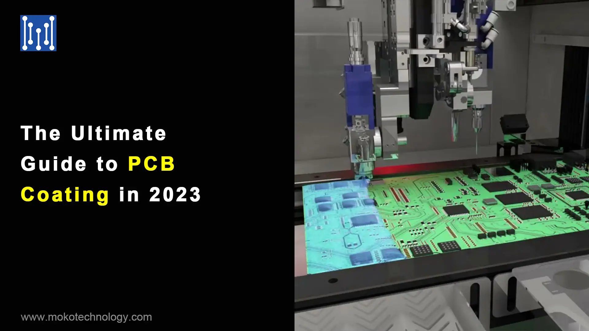
Proces powlekania PCB
Nałożenie powłoki ochronnej na płytki drukowane wymaga starannego przygotowania, podanie, odnalezienie, i testowanie:
- Przygotowanie powierzchni
Płyty należy dokładnie oczyścić przed nałożeniem powłoki, aby zwiększyć przyczepność. Typowe techniki obejmują czyszczenie rozpuszczalnikami i obróbkę powierzchni plazmą/koronowaniem.
- Aplikacja powłoki
Istnieją różne metody nakładania powłok na płytki drukowane, oni są:
- Opryskiwanie ręczne
Ta metoda jest odpowiednia dla serii niskonakładowych, ponieważ jest to proces czasochłonny. Normalnie, do nakładania powłoki używamy puszki z aerozolem lub ręcznego pistoletu natryskowego, i przed opryskiwaniem, te obszary, które nie wymagają malowania, muszą zostać pokryte. Efekty powlekania będą się nieco różnić między różnymi partiami ze względu na ręczną obsługę.
- Powłoka selektywna
Odnosi się do automatycznego procesu powlekania, który nakłada powłokę na określone obszary na płytkach drukowanych za pomocą zaprogramowanych zrobotyzowanych dysz rozpylających, i nie ma potrzeby zakrywania obszarów, które nie mają być spryskiwane. Proces ten charakteryzuje się wysoką wydajnością i dokładnością, nadaje się do produkcji wielkoseryjnej.
- Zanurzenie
Do tej metody, PCB byłyby najpierw zanurzane w roztworze do powlekania, a następnie usuwane. Na efekt powlekania wpływa wiele czynników, takich jak prędkość zanurzania i wyciągania, czas maczania, itp. Przed procesem powlekania wymagane jest rozległe maskowanie, więc nadaje się do tych płytek drukowanych, które wymagają powlekania po obu stronach.
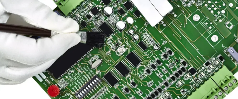
- Szczotkowanie
Pędzel służy do nakładania powłoki na określone obszary, i jest to metoda używana głównie do napraw i przeróbek. Proces zajmuje dużo czasu i wymaga dużo pracy, ostateczny efekt powlekania uzależniony jest od biegłości operatora.
- Utwardzanie/suszenie
Typowe metody utwardzania obejmują utwardzanie termiczne, Utwardzanie UV, i utwardzanie wilgocią. Ścisła kontrola procesu podczas utwardzania jest niezbędna, aby zapewnić całkowite usieciowanie powłok bez nadmiernej kruchości. Metodę utwardzania dobiera się tak, aby odpowiadała składowi chemicznemu polimeru oraz spełniała wymagania w zakresie wydajności i wydajności.
- Testowanie
Testowanie jest ważnym etapem sprawdzania zakresu wydajności i ograniczeń powłoki izolowanej obwodem w różnych warunkach środowiskowych w celu uzyskania pożądanych właściwości.
Idealna powłoka ma cechę nadmiernej przyczepności, dobre właściwości elektryczne, i właściwości fizyczne przy niskiej wilgotności. Te testy do testowania powłok obejmują zarówno testy podstawowe, jak i zaawansowane. Pierwszy, podstawowe testy sprawdzają przyspieszoną wilgotność i parametry elektryczne. druga, zaawansowane testy sprawdzają mgłę solną, szybka zmiana środowiska, i limit temperatury.
PCB Tablica Standardy powłok
W Powłoka ochronna, istnieje szereg standardów dotyczących powłok PCB, które wymagają ich stosowania w określonych warunkach, np. w wojsku, samochód, użytek krajowy, itp. Najczęściej powłoki ochronne kwalifikują się do specyfikacji MIL-I-46058C lub IPC-CC-830B, która jest ściśle związana z MIL-I-46058C.
MIL-I-46058C: Powszechny w branży standard powlekania konforemnego, znany również jako wojskowy związek izolacyjny. Wymaga testów w dowolnych laboratoriach autoryzowanych przez MIL i jest nadal używany nawet po dezaktywacji od 1998 dla nowych projektów. Ten test wymaga standardowej listy kwalifikowanych produktów (QPL).
Def Stan 59/47: Podobny standard do 46058C stosowany do powlekania wysokiej klasy urządzeń do użytku wojskowego, ale brytyjskie Ministerstwo Obrony musi je najpierw zatwierdzić.
IEC 61086: Standard oparty na samocertyfikacji przez dostawcę o podobnych wymaganiach do 46058c. Rządzi tym Międzynarodowa Komisja Elektrotechniczna.
IPC-CC-830B: Aktywnie używany i stale aktualizowany standard podobny do 46058C, wprowadzony, gdy 46058C pozostaje nieaktywny. Materiał znormalizowany dla 46058C zgodny z tymi specyfikacjami. Brak dostępnych testów, ponieważ nie jest utrzymywana QPL.
UL94V0: Odnosi się do właściwości samogasnącej powłoki ochronnej na podłożu FR4 FR. V0 to najwyższa osiągalna kategoria, której następcami są V1 i V2.