- Check that what you want can be manufactured. Apply design rules and check indicated violations.
- Check the layers stack.
- Check the board in 3D view to clean any obvious errors.
- Print 3D model and check with your mechanical designers.
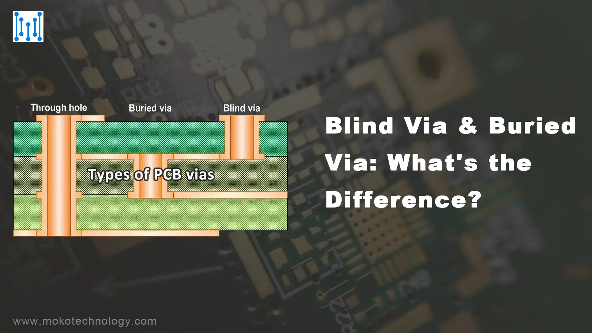
- Check the via diameters. Unify some of the hole diameters. Add more stitching to the polygons. Check that you have tenting where you want the solder mask cover. Modify paste rules to remove paste from test pads. Replace non-plated holes with board cutouts. Generate keep out layer.
- Check layout in single layers and in pairs.
- Generate and check Gerber layers of the single circuit.
- Check Gerber layers of the panelized board.
- Send the files to yourprocurement. Make sure that your attached comments and contact details are provided with the order and not removed by your purchasing guy. Get ready for the queries. Answer them back.
#PCBアセンブリ #PCB Dデザイン


