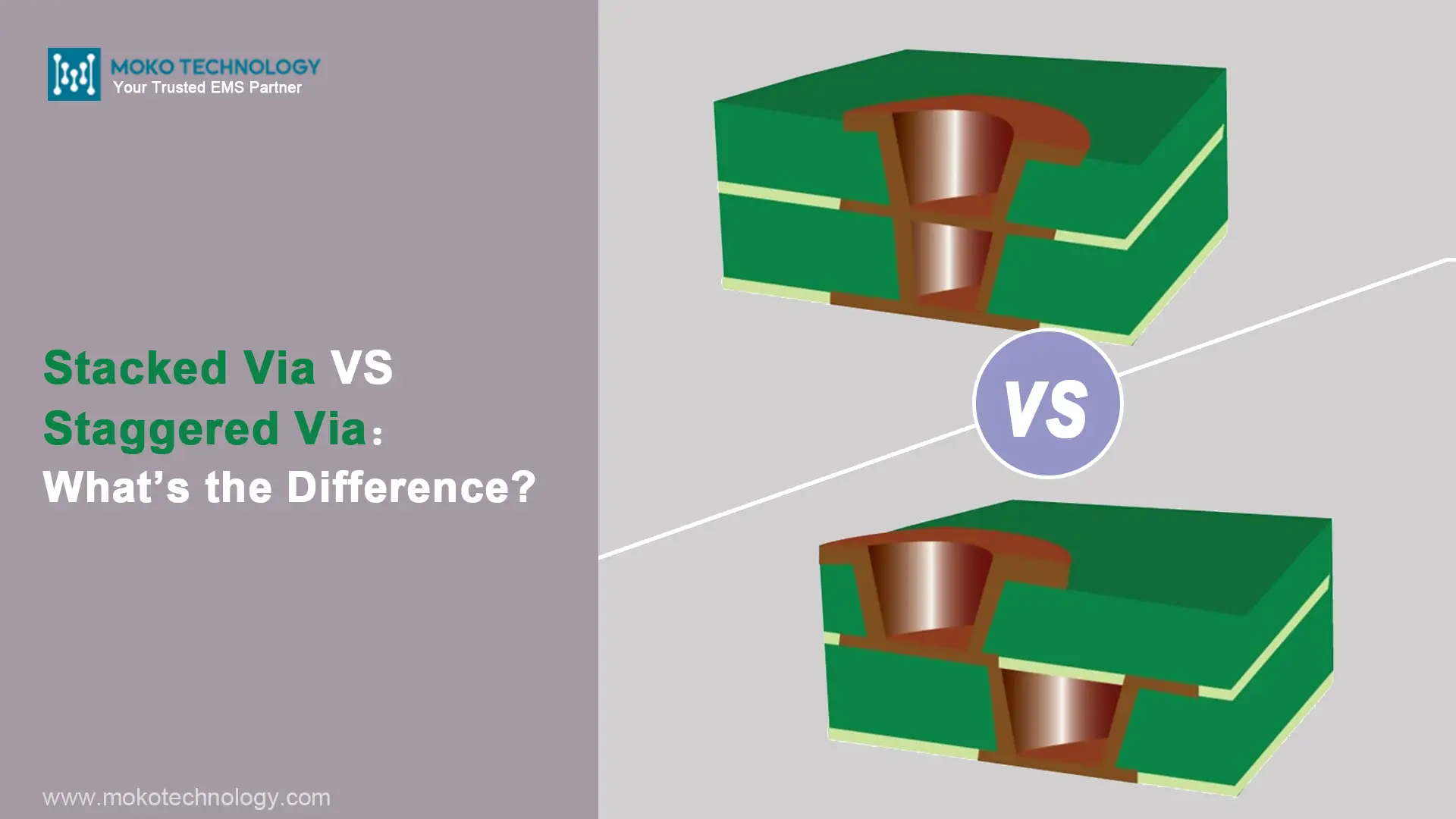
Is using a via to strengthen surface mount connector on the pad a good or bad practice?

I believe I have heard of putting a plugged via right next to a mechanical pad so that the board is stronger there. But I'm not sure what the implications are for putting a via on the pad?

There are some reasons for putting a via in the pad, but strengthening a connector is a new practice for me.

The weakest part of an SMD pad is that the copper could delaminate from the fiberglass, and lift off the PCB itself. Anything you could do to prevent that would help, including making the pad larger or putting a via in the pad itself.

But you have to be careful since putting a via in the pad can cause other issues.

  • The first problem is that it might make the pads not flat enough, so a connector pin won’t make good contact with the pad and thus not get soldered well.
  • The second issue is that the solder could get wicked down the via and leave nothing left for the connector pin. This isn’t a big issue if you are hand soldering, but can be a problem when doing it with automation.

Honestly, if connector strength is an issue, then it is advisable to seriously consider going to a through-hole connector or some type of connector, which gets strength from some other ways. Such as a connector that gets bolted to the chassis itself (and stress on the PCB is minimal).

Czytaj więcej: Montaż SMT

#PCB Design #PCB Assembly
Zdjęcie Olivera Smitha

Olivera Smitha

Oliver jest doświadczonym inżynierem elektronikiem specjalizującym się w projektowaniu płytek PCB, obwody analogowe, systemy wbudowane, i prototypowanie. Jego głęboka wiedza obejmuje ujęcie schematyczne, kodowanie oprogramowania sprzętowego, symulacja, układ, testowanie, i rozwiązywanie problemów. Oliver specjalizuje się w przeprowadzaniu projektów od koncepcji do masowej produkcji, wykorzystując swoje talenty w zakresie projektowania elektrycznego i zdolności mechaniczne.

O co pytają inni

Jakie są strony pierwotne i wtórne PCB?

I am designing a 2 layer PCB with components on both side of it. SMT components are one one side of PCB, but TH (through hole) components are on both sides. I need to understanding something mentioned by the supplier called primary and secondary sides.

Przeczytaj szczegółowe porady z artykułów na blogu

Przewiń na górę