В этом отрывке основное внимание уделяется базовым знаниям о паяльной маске LPI., например, его определение, важность, сравнение с другими масками, и попрактиковаться в применении.
Что такое паяльная маска LPI?
По факту, LPI solder mask is a mixture of two different liquids. Different from traditional epoxy inks, LPI is sensitive to ultraviolet light. In order to maintain their quality, factory usually saves them separately before using. But this does not stop it become one of the more cost-effective choices among other types. During manufacturing, people apply it on the surface of PCB for ultraviolet photolithography process after finishing viscous curing.
As customers, you have a variety color choices of LPI masks, including green, чернить, красный, желтый, белый, and blue. Безусловно, different colors have different visual effects. White solder mask provides high contrast and reduces glare against a green background glare. It makes the PCB look especially good and clean. Black solder mask, despite less contrast, is still easy to set off labels and large components. When it comes to red solder mask, it is so popular choice since it provides good visibility and contrast for flat surfaces and tracks. For Blue solder mask, it is very proper to use on heavy-label circuit boards, because it offers an obvious contrast with screen printing.
What Is LPI Solder Mask Made of?
Such a good mask must originate from its raw materials. It is made of light-cured resin, thermo-setting resin, photo-sensitive agent, thermo-curing agent, filler, color material, and other auxiliaries. With good photosensitive and thermal properties, the resin can be cured under specific conditions to form a stable protective mask. тем временем, the photosensitive agent enables the solder resistance film to carry a photochemical reaction and achieve local curing under lighting. Кроме, fillers and auxiliaries optimize the properties of the solder mask, including hardness, adhesion, и устойчивость к растворителям. This makes sure solder mask can effectively protect the PCB. All above greatly contributes to a perfect manufacturing process.
How Thick Is the LPI Solder Mask?
In order to fit product line, the ideal thickness of solder mask LPI is usually between 76.2 to 114.3μm, which can support the protection function of mask and maintain proper electrical performance. тем не мение, when we design the thickness of solder resistance film, we should also take factors like the property of the substrate material, the grind method, coating method as consideration. Only in this way, can we fulfill a smooth manufacture procedure.
What Is LPI Flex?
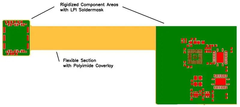
With the rapid development of flexible electronic devices such as wearable devices, LPI solder mask evolves into flex type accordingly. Similar as common LPI solder mask, people generally use liquid light imaging technique to make flex LPI mask on the circuit board. It takes advantage of photosensitizers and photocuring resins to precisely form pattern during exposure. It still inherits function like circuits protection from environmental corrosion as well as circuit stability enhancement.
Differing from common type, flexible LPI type is specially designed for the manufacture of flexible circuit boards. It is made of special materials with excellent flexibility, so it can adapt to the bending, folding and twisting pressure exerted against flexible circuit boards. In despite of good raw materials, we should not ignore the considerations like adhesion with the flexible substrate before batch production. This has great influence on tight bonding and stable performance between the solder mask and the flexible board.
Importance of LPI Solder Mask on PCB
LPI solder is very crucial in PCB manufacturing. It not only saves the board from various environmental and operational factors but also guarantees the reliability of the soldering process. Также, its precise image transfer ability further strengthens its application value.
Contaminant Prevention
LPI solder mask serves as a thin layer of polymer covering the circuit board. It mainly stop the copper from oxidation and short circuit during operation. Кроме, it is useful in keeping the board far away from dust and other contaminants, which results in short circuits. более того, it can isolate the board from moisture, mold and salt spray, leading to longer lifespan of the printed board.
Specific Protection
Soldering bridge is an unintended electrical connection which is likely to cause problems if used alone. Properly, solder mask LPI specifically offers a good solution to the point. It prevent bridge between the wire and the pad during components soldering through protecting the surface of the printed board.
Precise Image Transfer
LPI stands for liquid photogenesis Imaging and is an industry standard. The mask can be precisely transferred to the circuit board by spraying or screen printing in the form of ink. The precise printing allows better contact to PCB.
Double Curing
The LPI solder mask goes through double curing during its exposure to UV light to harden any exposed areas. This dual curing process enhances the durability and stability of the solder mask. If you are interested in how this technique matters a lot, feel free to visit our factory or свяжитесь с нами directly.
Ldi vs Lpi Solder Mask
Both LDI and LPI solder resist films is of great significance in the PCB manufacturing process. Both of them are solder mask that protect the copper on the circuit board from oxidation and short circuits in manufacturing. They all form a protective film on the circuit board through a specific process. But there are some obvious differences as follows.
They differ in how they work. Solder mask LPI mainly relies on photochemical reaction and thermal curing process to achieve its effect. It uses photosensitive agents and photo-curing resins to form precise patterns on the circuit board through steps, such as exposure and development. В отличие, ЛДИ (Laser Direct Imaging) solder mask relies on laser technology to form solder resist images directly on the circuit board. LDI technique adopts a high-resolution laser beam to illuminate the solder mask and cure it in a specific area to create specific pattern.
Кроме того, LPI and LDI differ in terms of cost and efficiency. LPI solder mask is generally a cost-effective option in batch PCB manufacturing because of its high accuracy and rapid imaging characteristics.
How to Apply LPI Solder Mask
First step is coating process. LPI solder resistance film is coated to the etched PCB substrate by curtain coating or screen printing. This step makes sure that the solder mask is evenly covered on the circuit board. Второй, we are going to pre-drying after coating. The purpose of pre-drying is to remove part of the solvent and to make the solder mask cured. Next step is exposure. By lithography, LPI solder mask is exposed to a specific area of UV light produced by UV laser. потом, Photochemical reactions occur in these areas to form a pattern, following by development process. Un-illuminated areas will be removed during development process, leaving the exposing areas ready for soldering and other surface treatment. In final, we come to post-curing. The solder mask are completely cured to form a stable protective film under heat treatment.
LPI Solder Mask Application
Подводить итоги, PCB LPI solder mask is able to protect the circuit from environmental damage as well as prevent electrical faults during soldering. It also has excellent adhesion and solvent resistance. Such excellent features contribute to its wide application. LPI solder mask is used in the field of electronics manufacturing, especially in the manufacturing process of printed circuit boards. It is also suitable to manufacture of flexible circuits due to its good flexibility and adaption to the bending board.
