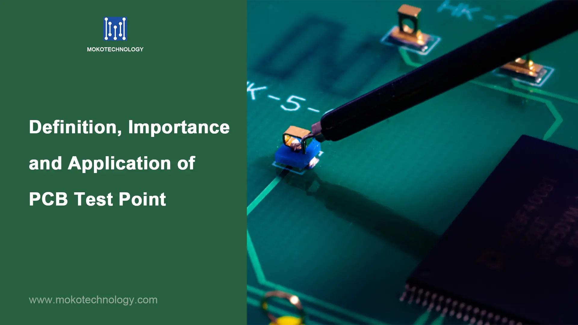
Хотя точка тестирования печатной платы кажется маленькой, он отлично работает. В этом блоге мы углубимся в определение, важность, дизайн, и применение контрольной точки печатной платы. We hope this is helpful to you.
What Is A Test Point on A PCB?
Прежде всего, we need to know what a test point is. По сути, the function of the test point is to test whether the components on the circuit board meet the specifications and solderability. Test points contain sockets, булавки, и разъемы, detecting various electrical signals and power supplies.
We should choose the proper type of test point according to our practice requirements. Например, signal test point needs a socket or pin type, while the power test point needs connector type.
There are commonly three types of test points you need to know. Первый, integrated test points refer to placing test points under or around components of a circuit so that they can be easily tested when needed. So it can be coded directly in the PCB layout design, which is a good way to avoid the use of additional circuit elements.
The second type is socket and pin test points, which are very frequently used. You just need to fix the socket or pin on the PCB board and connect it with the circuit. Both socket and pin test points have the advantages of high reliability and small space.
В третьих, connectors are one of the most common test point types. It makes it easy to connect the test equipment to the PCB board during testing. Connector test points are generally used to connect power and signal, with high reliability and long service life. тем не мение, it occupies a large space.
Why Test Points Are Important for PCB Manufacturing?
Is it necessary for each PCB to add test points? The answer is absolutely yes. It is unlikely to use an electric meter to check every IC, резистор, capacitor and inductor one by one. Следовательно, ИКТ (in circuit test) shows great advantages to handle this situation in a efficient way. It can save a lot time by simultaneous contact to all test points of the board by multiple probesIts test automation mainly depends on a program control system which priors to sequence then to parallel order.
тем не мение, if the probe of machine directly touches the electronic parts on the board or its welding feet, it likely results in component damage. Таким образом, the invention of test point is particularly important.
Test points are located at the two ends of components, without a mask. They allows the test probe to reach the circuit without directly touching the electronic part being measured.
How do We Design Test Points in PCB Board?
If we want to add some test points in PCB design, what should we take care of? Первый, we should decide the amount and location of the test points on the PCB. Второй, it is not good to set the PCB test points on the surface where electronic devices need to be installed. тем временем, in order to ensure the connectivity of the test point, you would look after the interface between test point and board as well as the installation of the connector. В третьих, the test points should conform to certain layout rules. Например, when designing PCB routing, the test points can be concentrated in the same logical or functional places. В письме, reasonable test point settings are capable of testing, debugging, maintenance and other aspects of the work.
How to Connect to PCB test Points
Безусловно, if products are going to the automatic testing process, we don’t have to checking the PCB by manual one by one. тем не мение, if you now are just in the process of making PCB samples, the following step-by-step guidance will help you a lot.
- Ensure that the circuit board is powered off and appropriate ESD measures are in place. This greatly prevents electrostatic damage to electronic components.
- Select the right PCB probe according to the test program. The choice of probe depends on the type of interface on the PCB and the parameters which will be measured.
- Insert the PCB probe into the test point or pad on the PCB, for effective connection.
- Measurement parameters Select.Use an measuring device as required, such as a multi-meter or oscilloscope, and then connect it to the PCB probe.
- Perform measurement. Testing of Measure voltage, текущий, signal waveform and other parameter sare available.
Where to Use Test Points
Somebody may also has a question on where test points are applied. Based on our experience, they mainly use in two type of test for PCB.
Внутрисхемный тест (ИКТ)
PCBA ICT is the most powerful and popular PCBA testing method for high volume and mature products. Также, it is widely trusted and used by many PCB manufacturers and customers. It can realize ninty-five percent accuracy.
During PCBA ICT, an electrical probe with nail bed input current to test points on PCB. Nail tester bed just press the PCB over the probe bed to make a firm connection for testing. Surely, these test points are pre-designed on the circuit board to allow the contact of ICT. These tests are used to verify the position, ориентация, and function of every electronic component on the PCB. It is capable of detecting problems such as short circuit, open circuit, сопротивление, емкость. Each coins has two sides. For large product batches, you have to customize fixture for faster and more efficient in-circuit testing. Это, to some degree, is costly, depending on considerations like board and fixture size.
Тест летающего зонда (ФПТ)
Similar to ICT, flying probe тестирование is often seen as an upgrade version. In addition to the PCB test points, flying probe machine can enter uncovered through-holes. Кроме, it can be programmed to check the value of orientation of the diode transistor, the passive component, and voltage. It can be quickly, easily and economically adapted to new circuit boards through simple programming modifications. This test method are suitable for both small batch production tests and prototype tests, while it is less cost-effective for mass production.


