マスクレイヤーを貼り付けます, 上層と下層の両方, THTコンポーネントに必要?

I know the paste mask layer is also called the stencil layer. It's only used for assembly. I want to know if the paste mask layer (上層と下層の両方) is necessary for through hole components. For SMD components I know the paste mask layer is required to solder the components. Is it necessary for through hole components?

番号. Paste mask is normally used only for reflowing surface mount components, while the through hole components are soldered either manually or by wave solder bath at a later stage.

If you have through hole parts and the surface mount components on the bottom side, the paste mask stencil is not required, as the parts will all be soldered at once in a wave solder bath. This process requires you to generate a glue dot coordinates file, which will be used to place a dot of glue under the surface mount component and that will keep the part in place during the soldering process.

If the only through hole parts in the PCB were the connectors, it is also possible to reflow through hole components with solder paste. That requires some tweaking to get the right pad size and stencil opening. All we need to do is to have a larger pad on the top side, so that there was enough paste on the pad to wick down the hole and ensure a solid solder joint.

続きを読む: THTPCBアセンブリ

#PCBアセンブリ
の写真 オリバー・スミス

オリバー・スミス

オリバーは、PCB 設計に熟練した経験豊富なエレクトロニクス エンジニアです。, アナログ回路, 組み込みシステム, とプロトタイピング. 彼の深い知識は概略図のキャプチャに及びます, ファームウェアコーディング, シミュレーション, レイアウト, テスト, そしてトラブルシューティング. オリバーは、電気設計の才能と機械の適性を活かして、プロジェクトをコンセプトから量産まで進めることに優れています。.
の写真 オリバー・スミス

オリバー・スミス

オリバーは、PCB 設計に熟練した経験豊富なエレクトロニクス エンジニアです。, アナログ回路, 組み込みシステム, とプロトタイピング. 彼の深い知識は概略図のキャプチャに及びます, ファームウェアコーディング, シミュレーション, レイアウト, テスト, そしてトラブルシューティング. オリバーは、電気設計の才能と機械の適性を活かして、プロジェクトをコンセプトから量産まで進めることに優れています。.

他の人が尋ねていること

低周波デジタルロジックシステムではバイパスコンデンサを外したままにしてもよいでしょうか?

IC の電源ピンの近くにバイパス コンデンサを使用することをお勧めします。, しかし、現在はブレッドボードの段階から PCB の設計段階に移行しています。, そして、キャップが実際に必要な場合についての適切な経験則があるかどうか知りたいです.

メーカーから PCB を印刷してもらい、SMT を自分の機械で行うことを検討しています。. それは良い考えだと思いますか?

私が計画を立てている理由は、必要があるからです 50-100 回路基板は数週間ごとに作成され、PCB 印刷のコストは安くなりますが、PCBA SMT は膨大です. メーカーが料金を請求するため $400 あらゆる新しいデザインに. そこで、自分でできるように機械を購入しようと思いました. そういった経験がないので意見を聞きたいです.

ブログ記事から詳細なアドバイスを読む

PCB と PCBA: 違いは何ですか
ウィル・リー

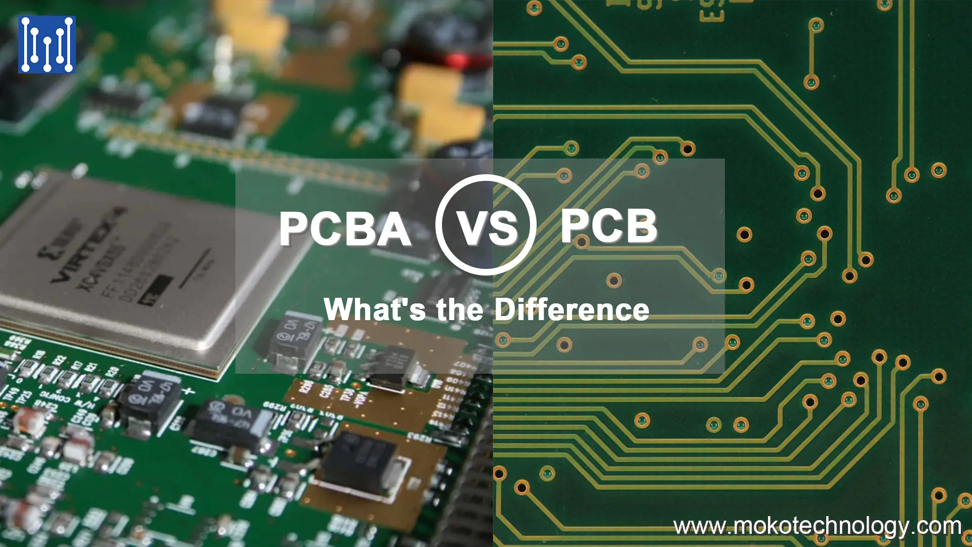
PCB と PCBA: 違いは何ですか?

PCB と PCBA はエレクトロニクス業界で最も一般的な 2 つの用語です. たった一文字の違いなのに, それらは異なるものを表します

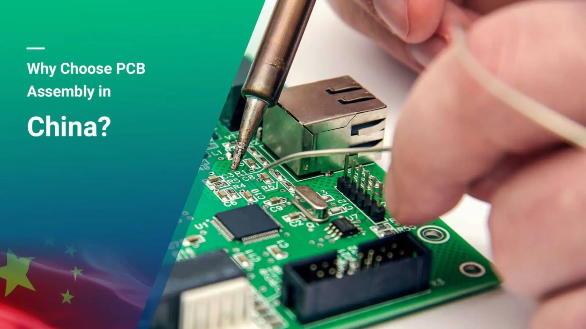
中国でPCBアセンブリを選ぶ理由
ウィル・リー

中国でPCBアセンブリを選ぶ理由?

プリント回路基板 (PCB) 組み立てはエレクトロニクス製造において不可欠なステップです. これには、電子コンポーネントをベア PCB ボードにはんだ付けして組み立てて、機能的なものを作成することが含まれます。

トップにスクロールします