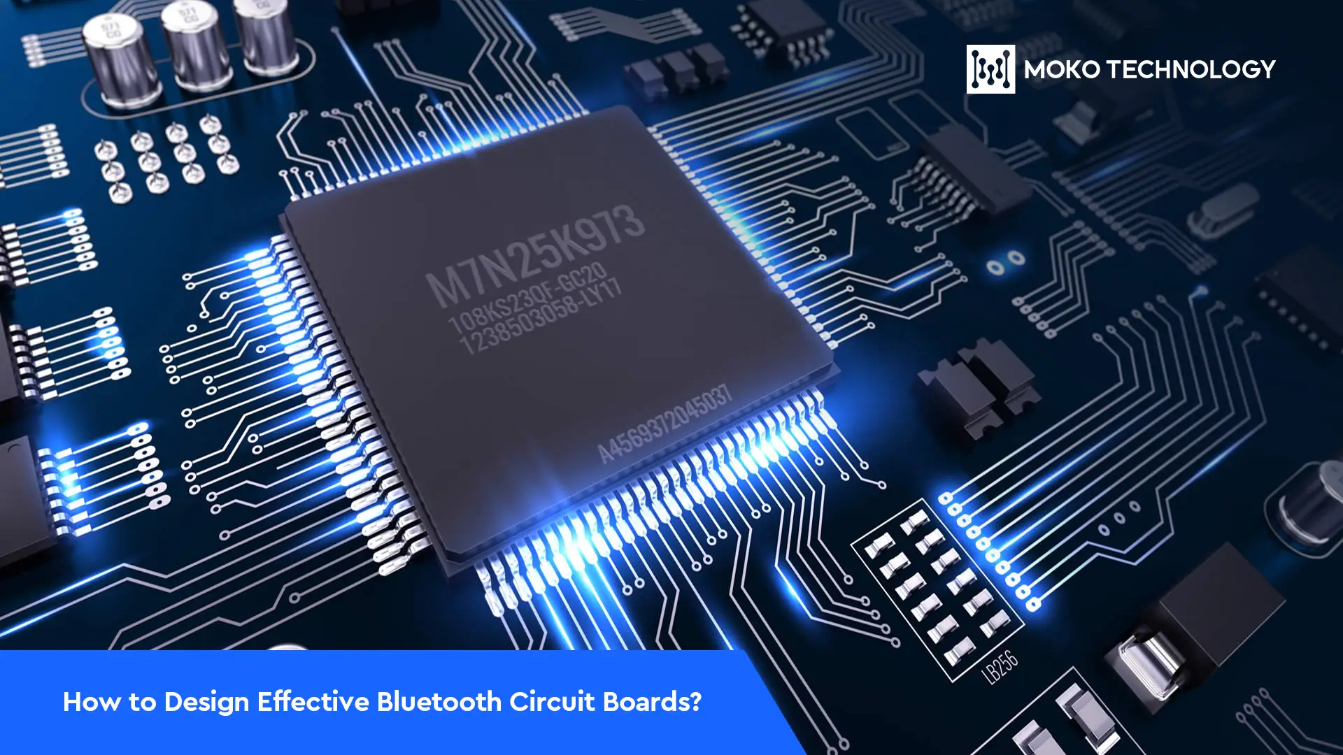
Il Bluetooth è ovunque al giorno d'oggi! Lo si può trovare in smartphone, cuffie, altoparlanti: praticamente qualsiasi dispositivo che si connette in modalità wireless probabilmente utilizza il Bluetooth. Quindi, quando si progetta un nuovo prodotto elettronico che necessita di funzionalità wireless, aggiungere il Bluetooth di solito ha senso. Per farlo, in genere è necessaria una scheda Bluetooth progettata su misura. In questo articolo del blog, forniremo indicazioni per una progettazione efficace di schede PCB Bluetooth. Per iniziare, introdurremo le conoscenze fondamentali sulle schede Bluetooth.
Comprendere i circuiti stampati Bluetooth
Per prima cosa, rivediamo come Tecnologia Bluetooth Funziona. Il Bluetooth sfrutta le frequenze radio per consentire la comunicazione tra dispositivi. Operando a 2.4 GHz, può abilitare connessioni wireless simili ad altri standard come il Wi-Fi. La portata effettiva va da 1 centimetro a 100 metri. Un aspetto importante del Bluetooth è che i dispositivi devono associarsi e stabilire un codice univoco autorizzato prima di poter scambiare informazioni. Inoltre, l'hardware dotato di Bluetooth può risparmiare energia entrando in modalità standby quando non sta trasmettendo dati attivamente.
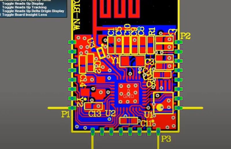
Una scheda PCB Bluetooth si riferisce specificamente al circuito stampato che abilita le funzionalità Bluetooth. Contiene un modulo o chip Bluetooth, un'antenna per la trasmissione/ricezione dei segnali, un microcontrollore per l'elaborazione dei dati wireless e componenti di supporto come condensatori, resistori e transistor. Il modulo Bluetooth contiene il ricetrasmettitore radio insieme a un controller di banda base, stack di protocollo, firmware di interfaccia e altro ancora. Un posizionamento di qualità dell'antenna sul PCB garantisce una buona portata wireless tra i dispositivi connessi. È necessaria un'attenta progettazione del circuito per gestire il consumo energetico mantenendo al contempo la larghezza di banda necessaria per le velocità di trasmissione dati previste dall'applicazione.
Applicazioni dei circuiti Bluetooth
La tecnologia Bluetooth consente la connettività wireless per una vasta gamma di applicazioni, tra cui:
- Beacon per la vendita al dettaglio per il rilevamento della posizione
- Raccolta dati di sensori industriali
- Prodotti audio come cuffie wireless
- Controller di gioco e periferiche per computer
- Sistemi di controllo domotico
- Fotocamere, stampanti, telefoni ed elettronica di consumo
Pur sfruttando lo stesso protocollo Bluetooth di base, l'implementazione e l'ottimizzazione variano notevolmente tra queste applicazioni, a seconda della velocità dei dati, delle modalità di connettività, della portata operativa e delle esigenze di affidabilità del caso d'uso.
Rispetto al Wi-Fi, il Bluetooth offre velocità di picco inferiori e una portata più limitata, soprattutto attraverso muri o altri ostacoli. Tuttavia, la versione 5.0 offre una velocità di trasmissione migliorata rispetto alle versioni precedenti. È importante sottolineare che il Bluetooth mantiene un consumo energetico relativamente basso, protezioni di sicurezza, supporto per piccole periferiche e ampia compatibilità.
Durante lo sviluppo di un PCB abilitato Bluetooth, gli ingegneri prendono diverse decisioni progettuali per rafforzare l'integrità del segnale e ridurre al minimo le interferenze/perdita di pacchetti per la loro applicazione. In seguito, forniremo alcuni spunti per ottimizzare le prestazioni delle schede a circuito stampato Bluetooth.
Considerazioni e suggerimenti per la progettazione di schede PCB Bluetooth
- Usa moduli certificati
L'utilizzo di un modulo Bluetooth pre-certificato di fornitori come Microchip o Silicon Labs semplifica l'integrazione integrando radio Bluetooth, antenna sintonizzata, stack firmware e microcontrollore in un'unica soluzione autonoma. I moduli vengono sottoposti ai test e alle certificazioni richiesti dagli enti regolatori per ridurre il carico di lavoro dei team di progettazione. Inoltre, consentono un time-to-market più rapido eliminando la complessità dei layout RF e della sintonizzazione dell'antenna. I moduli certificati più comuni sono dotati di processori ARM integrati per gestire le comunicazioni Bluetooth e controllare le periferiche I/O tramite pin GPIO, SPI, I²C e PWM.
- Posizionare con attenzione l'antenna
L'antenna che consente la connettività wireless deve essere posizionata con cura sul bordo della scheda, racchiusa in un vano RF in plastica, se possibile. Eventuali piani in rame nelle vicinanze, PCB tracce, pad o colate poligonali possono degradare le prestazioni RF, motivo per cui i fornitori di chip Bluetooth forniscono linee guida dettagliate per il layout. Queste richiedono aree di spazio libero sugli strati sopra e sotto la sezione dell'antenna fino ai bordi della maschera di saldatura. I via che uniscono gli strati di segnale a terra aiutano a contenere le radiazioni. Modellare la scheda per posizionare un'antenna Bluetooth a un'estremità o in un angolo la separa dagli altri componenti elettronici.
- Mitigazione delle interferenze
Poiché il Bluetooth utilizza la banda di frequenza a 2.4 GHz, un canale affollato, le interferenze provenienti da altri segnali wireless possono interrompere la connettività e ridurre la velocità dei dati. Tra le fonti di interferenza figurano router WiFi, dispositivi Zigbee, forni a microonde, apparecchiature video wireless e altri dispositivi che condividono le stesse frequenze. È importante valutare attentamente l'ambiente in cui opererà la scheda PCB Bluetooth e, ove possibile, posizionarla lontano da radio che notoriamente generano interferenze. Un'ulteriore schermatura attorno all'antenna, componenti di filtraggio del rumore e tecniche software possono contribuire a mitigare i problemi di interferenza.
- Consumo di energia
Il Bluetooth è stato progettato per consumare meno del Wi-Fi, ma deve comunque essere ottimizzato per un'autonomia accettabile della batteria. Sviluppare budget di potenza dettagliati del sistema stimando le modalità di utilizzo, i cicli di trasmissione/ricezione, il tempo di ascolto inattivo e così via. Selezionare moduli e microcontrollori Bluetooth a basso consumo, utilizzare modalità di risparmio energetico tra le trasmissioni di dati, ridurre al minimo i tempi di attività e tecniche simili per estendere il funzionamento con una singola carica. La progettazione del PCB dovrebbe evitare percorsi di dispersione e garantire che ai componenti Bluetooth venga fornita energia pulita e stabile.
- Vincoli di dimensioni fisiche
Quando si progetta un dispositivo Bluetooth con PCB che deve essere portatile, è necessario considerare i limiti di dimensioni fisiche. L'involucro in cui il dispositivo verrà inserito impone vincoli sulle dimensioni complessive del PCB. Inoltre, poiché il dispositivo probabilmente dovrà integrare componenti per svolgere altre funzioni oltre alla connettività Bluetooth, lo spazio sul PCB deve essere gestito con attenzione. Scegliere attentamente le dimensioni e la posizione del package dei chip può contribuire a ottimizzare l'utilizzo dello spazio disponibile.
- Considerare le interferenze del mondo reale
Materiali di uso quotidiano come acqua e oggetti metallici ostacolano facilmente le onde radio Bluetooth, anche a brevi distanze di 1-2 metri. Microonde, Wi-Fi e altri dispositivi elettronici di consumo congestionano la banda a 2.4 GHz. L'inclusione delle antenne in schermature metalliche degrada ulteriormente la connettività. È previsto un rapporto inverso della perdita di segnale al quadrato in base alla distanza. Per compensare, utilizzare un'antenna con guadagno più elevato o velocità di trasmissione dati inferiori. I test dei prototipi in ambienti operativi reali determinano le necessarie misure di mitigazione delle interferenze.
- PROVE E CERTIFICAZIONI
Testare attentamente il progetto del PCB Bluetooth in una vasta gamma di ambienti operativi e condizioni d'uso è fondamentale, prima di implementarlo in produzione. È necessario testare diverse posizioni e orientamenti della scheda e delle fonti di interferenza esterne per qualificare la portata e la velocità wireless. È inoltre necessario garantire la compatibilità con gli stack software e i sistemi operativi dei dispositivi di destinazione durante l'integrazione. Infine, è necessario inviare il progetto a Bluetooth SIG per la qualificazione completa e il branding dei prodotti finali.
Ulteriori letture: Perché è necessario il test PCB?
Conclusione
La tecnologia wireless Bluetooth continua a progredire per potenziare sempre più applicazioni e dispositivi embedded. L'integrazione della connettività Bluetooth introduce complessità di progettazione hardware e software per ottenere le migliori prestazioni, dalla selezione dei componenti al posizionamento dell'antenna fino alla mitigazione delle interferenze. Seguire le linee guida sui moduli certificati, l'isolamento dell'antenna, l'ottimizzazione della potenza, i test di affidabilità ambientale e la certificazione finale crea un processo di sviluppo efficace. Grazie a queste informazioni su fattori chiave nella progettazione di schede a circuito stampato Bluetooth, gli ingegneri possono sfruttare appieno le funzionalità Bluetooth per un controllo wireless affidabile, comunicazioni, aggiornamenti e altro ancora nei loro prodotti di nuova generazione.