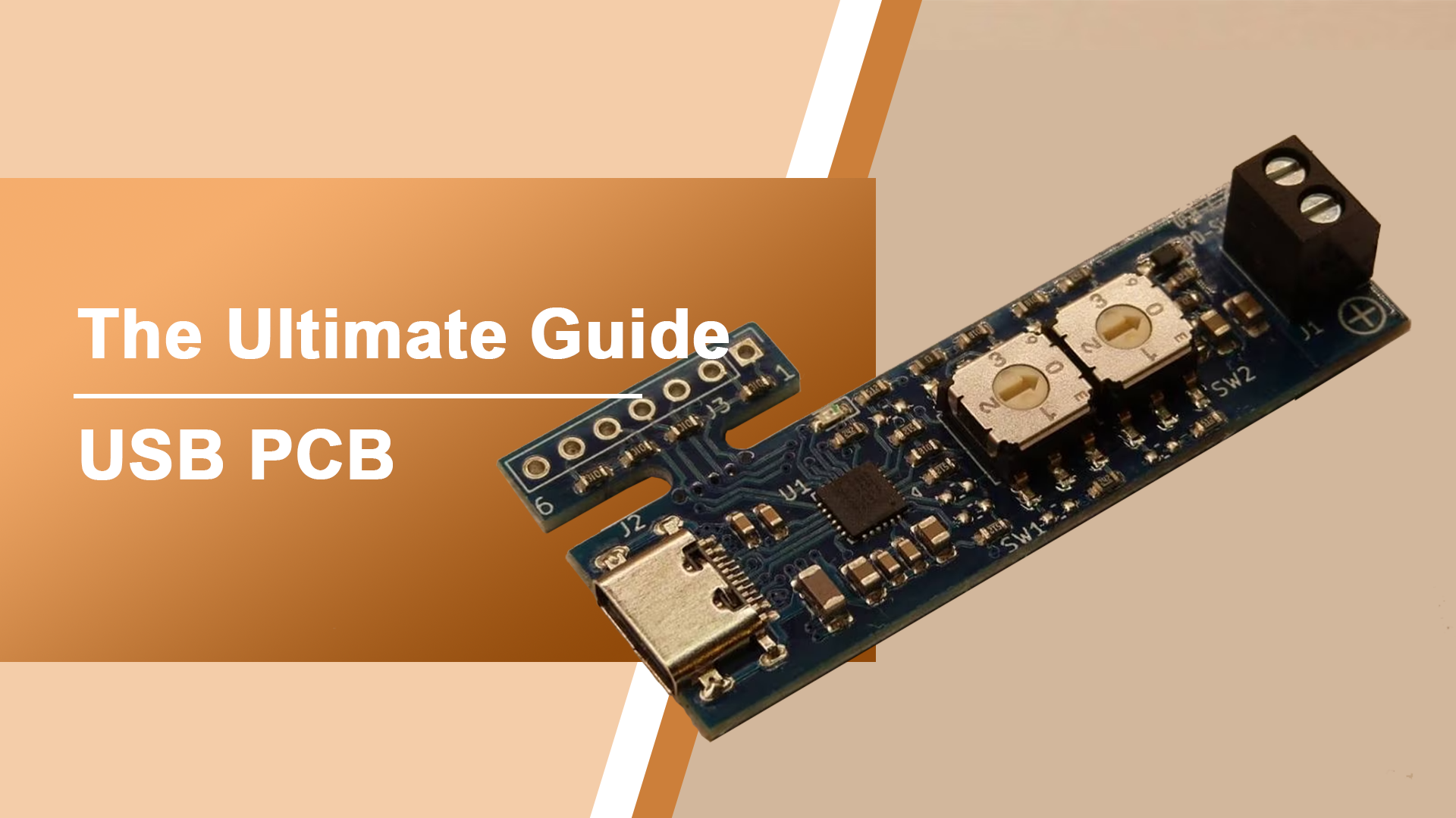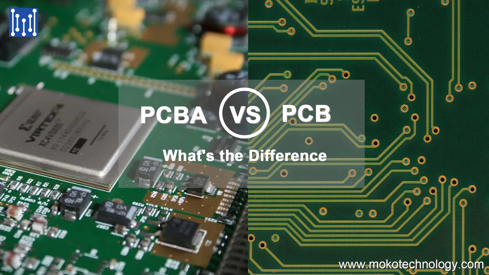
PCB y PCBA Son los dos términos más comunes en la industria electrónica. Aunque solo se diferencian en una letra, representan cosas distintas. El nombre completo de PCB es "placa de circuito impreso", que se refiere a una placa en blanco sin componentes electrónicos ensamblados. PCBA significa "ensamblaje de placa de circuito impreso", que se refiere a una placa ensamblada con varios componentes y capaz de realizar ciertas funciones. PCBA se basa en PCB. En este blog, los presentaremos por separado y compararemos sus diferencias en detalle.
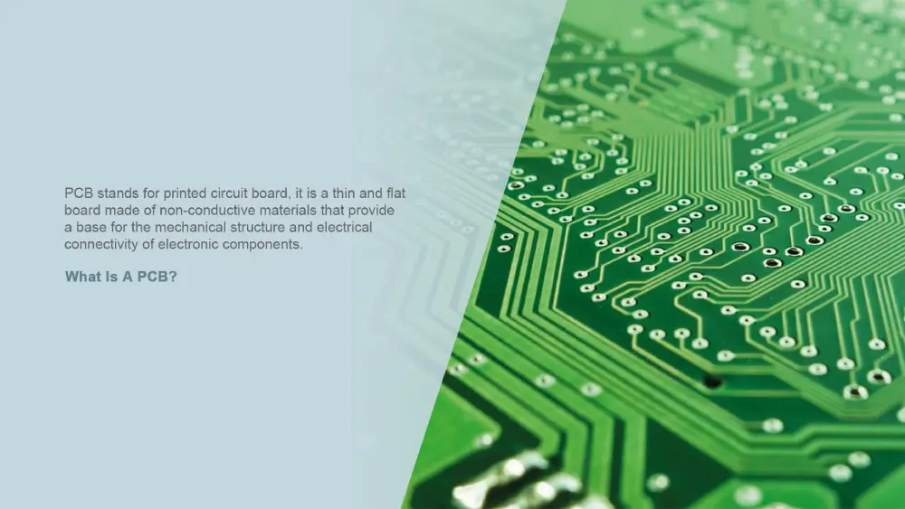
¿Qué es una PCB?
Una PCB (placa de circuito impreso) es una placa delgada y plana hecha de materiales no conductores. Sirve como base para el soporte mecánico y la conectividad eléctrica de los componentes electrónicos. Sustratos de PCB, generalmente hechas de materiales no conductores como fibra de vidrio o resinas epoxi, permiten el grabado o la impresión de vías conductoras de cobre sobre su superficie. Estas vías de cobre se conocen como trazas y conectan eléctricamente varios... componentes de la placa de circuito que están soldados a la PCB.
¿Cuáles son los diferentes tipos de PCB?
Según el número de capas conductoras de cobre se puede clasificar en:
PCB de una cara tienen pistas de cobre en un solo lado del sustrato aislante, ofreciendo soluciones simples y de bajo costo para circuitos básicos.
PCB de doble cara tienen pistas conductoras en ambos lados del sustrato, lo que permite diseños más compactos que los PCB de una sola capa.
PCB multicapa Tienen múltiples capas de cobre unidas, lo que permite circuitos mucho más densos y complejos. Son ideales para electrónica avanzada y permiten señales de alta velocidad.
Según los diferentes materiales utilizados, las placas de circuito impreso también se pueden clasificar como PCB de metal, Placa de circuito impreso fr4, PCB de cerámica, etc.
Para conocer más sobre los tipos de PCB, fMás lecturas: ¿Cuántos tipos de PCB existen?
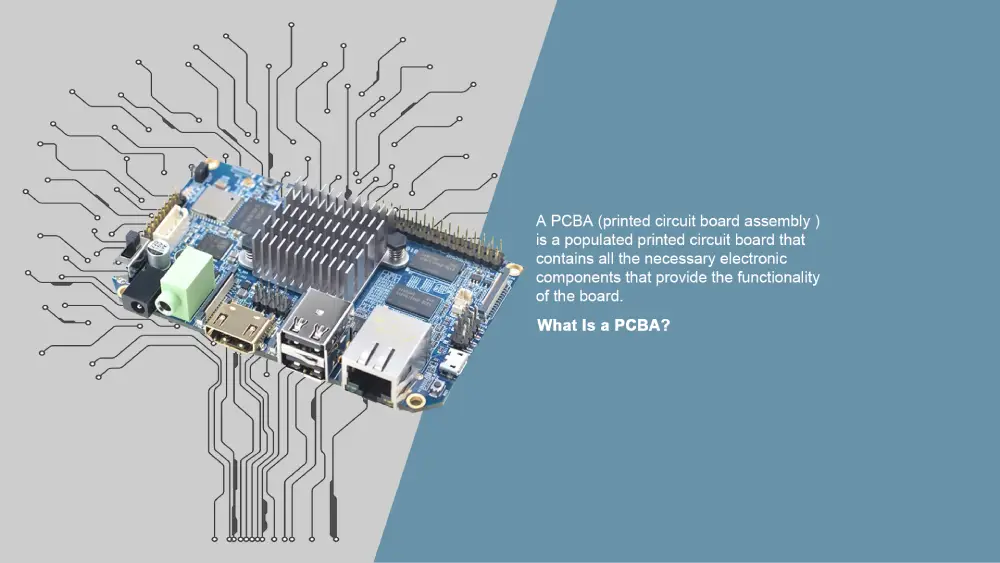
¿Qué es una PCBA?
Un PCBA (ensamblaje de placa de circuito impreso) se refiere al resultado de soldar todos los componentes electrónicos necesarios en una placa PCB en blanco, lo que permite que la placa ensamblada se convierta en un circuito completamente funcional. Además, también indica el proceso de instalación de los componentes en la placa de circuito.
Tres principales PCB Aensamblaje Métodos
La mayoría de los fabricantes de PCBA utilizan tres métodos para el ensamblaje de PCB. A continuación, se presenta una breve introducción.
Tecnología de montaje en superficie (SMT)
SMT es un proceso automatizado que puede montar directamente componentes de montaje en superficie Se instalan sobre la superficie de la PCB sin necesidad de taladrar. Estos componentes SMT son pequeños y se pueden compactar para lograr una placa de circuito compacta.
Tecnología de orificio pasante (THT)
THT es un método que consiste en insertar componentes con pines en orificios perforados en la placa de circuito impreso (PCB). Los cables que sobresalen se sueldan en el lado opuesto. Estos componentes THT son grandes y requieren ensamblaje manual.
Tecnología mixta
La tecnología mixta combina las ventajas de SMT y THT. Permite soldar SMT pequeños y grandes. Componentes THT en el mismo PCB.
¿Cuál es la diferencia entre PCB y PCBA?
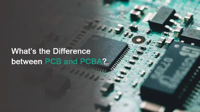
Aunque a menudo se usan indistintamente, PCB y PCBA representan diferentes etapas de la fabricación de productos electrónicos. Para aclarar la confusión entre ambos, explicamos aquí sus cinco diferencias principales.
1. Composición y función
En cuanto a PCB, se compone principalmente de estas 4 capas:
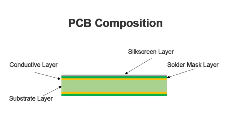
- Los substrar layer Generalmente está hecho de FR-4, que proporciona rigidez y aislamiento.
- Capas delgadas de lámina de cobre están unidos al sustrato para formar caminos conductores para la señal.
- Thcapa de máscara de soldadura electrónica Es un recubrimiento de polímero protector que evita cortocircuitos y corrosión dejando expuestas las aberturas soldables.
- La capa de serigrafía Con etiquetas impresas, proporciona instrucciones de montaje y colocación de componentes.
En cuanto a PCBA, es una unidad funcional completa, que incluye:
- PCB Sirve como base y está listo para instalar componentes.
- Componentes electrónicos Por ejemplo, los condensadores, transistores y resistencias se montan en la placa con SMT o THT y cada uno cumple distintas funciones.
- Traces Son canales conductores delgados en la superficie de la PCB para transportar señales eléctricas.
- Vía Son pequeños orificios perforados en la PCB para unir varias capas en las PCB multicapa, lo que permite que las señales se transmitan entre ellas.
- Soldadura pastas forma enlaces eléctricos y mecánicos.
2. Proceso de manufactura y máquinas requeridas
Otra diferencia importante entre PCB y PCBA es su proceso de fabricación:
PCB Proceso de manufactura
La fabricación de PCB gira en torno a la elaboración de la placa de circuito desnuda El proceso de fabricación suele estar automatizado y caracterizado por una alta precisión, utilizando máquinas especializadas.
- Los diseñadores utilizan software de diseño de PCB (por ejemplo, Altium, Cadence) para ayudar a diseñar el diseño.
- El cobre no deseado se elimina mediante máquinas de grabado para formar trazas y se aplican capas de cobre al sustrato mediante prensas de laminación.
- Las máquinas de perforación CNC y los taladros láser crean vías y orificios pasantes en la placa.
PCBA Proceso de manufactura
El PCBA parte de la placa de circuito impreso (PCB) para integrar los componentes electrónicos. Este proceso de ensamblaje puede ser manual o automatizado, y requiere diferentes equipos para un montaje eficiente de los componentes.
- Las impresoras de pasta de soldadura aplican cantidades precisas de pasta de soldadura sobre las almohadillas de PCB.
- Las máquinas pick-and-place automáticas y de alta velocidad aplican los componentes SMD con alta precisión utilizando brazos robóticos.
- Los hornos de reflujo funden la pasta de soldadura con un perfil térmico controlado, consolidando conexiones resistentes. El equipo de soldadura por ola se utiliza para componentes con orificio pasante.
3. Defectos
Dado que los procesos de fabricación de PCB y PCBA son diferentes, los posibles defectos que presentan también varían. Las PCB pueden presentar estos defectos: exceso o falta de cobre, grabado excesivo o insuficiente, falta de orificios perforados, aberturas y cortocircuitos. Las PCBA pueden presentar defectos como componentes faltantes o desalineados, exceso de soldadura, puentes de soldadura, etc.
4. Pruebas
Una PCB desnuda debe someterse a una verificación eléctrica antes del ensamblaje. La prueba de fijación consiste en usar una fijación especial de clavos con sondas que se conectan con precisión a los nodos de prueba de la PCB para probar el circuito. También se puede usar para probar las almohadillas de la PCB, lo cual es un método de prueba más eficiente. En la prueba de sonda flotante, una sonda móvil y flexible contacta los puntos de prueba.
Una PCBA necesita verificar sus componentes, soldadura, funcionalidad y fiabilidad a largo plazo. La prueba en circuito (ICT) se utiliza para detectar componentes de PCB mediante un dispositivo de fijación, lo que facilita la detección de fallos de fabricación. La prueba de sonda flotante también puede utilizarse para detectar PCBA. La prueba funcional simula las condiciones reales de funcionamiento de la PCBA para comprobar su funcionamiento normal. La prueba de envejecimiento simula el funcionamiento periódico y a largo plazo para evaluar su durabilidad y estabilidad. Una prueba en entornos hostiles expone la placa ensamblada a temperaturas extremas, humedad, caídas o vibraciones.
5. Tiempo de producción y Costo
La fabricación de PCB suele ser más rentable y eficiente en términos de tiempo que el ensamblaje de PCB. Los costos de PCB son menores debido a un diseño más simple y al gasto en materiales. El PCBA implica mayores costos de componentes y procesos de ensamblaje que requieren mucha mano de obra. Además, los plazos de entrega de PCBA son más largos debido a la integración de componentes y a las exhaustivas pruebas requeridas.
| técnicos | PCB | PCBA |
| Definición | Una placa de circuito desnuda sin componentes | Una placa de circuito completamente ensamblada con todos los componentes necesarios |
| Componentes | Ninguna | Todos los componentes necesarios están ensamblados. |
| Función | Como base para el ensamblaje de componentes electrónicos | Como módulo electrónico completo listo para funcionar |
| Proceso de fabricación | Diseño de la disposición de PCB, grabado de trazas de cobre, adición de capas aislantes y perforación de orificios. | Aplicación de pasta de soldadura, colocación de componentes y soldadura. |
| Máquinas requeridas | Software de diseño, máquinas de grabado, prensas de laminación, taladradoras CNC y taladradoras láser | Impresoras de pasta de soldadura, máquinas de selección y colocación, hornos de reflujo y máquinas de soldadura por ola |
| Técnicas de montaje | No es necesario, ya que no hay componentes instalados | SMT, THT y tecnología mixta |
| Métodos de empaque | Envasado al vacío | Embalaje con compartimentos o embalaje antiestático |
| Defecto de manufactura | Exceso o falta de cobre, grabado excesivo o insuficiente, orificio perforado faltante, aberturas y cortocircuitos | Componentes faltantes o desalineados, exceso de soldadura, puentes de soldadura |
| Pruebas | Prueba de fijación, prueba de sonda volante | Prueba de TIC, prueba funcional, prueba de sonda volante, prueba de envejecimiento, prueba en entornos hostiles |
| Costo | Más Bajo | Más alto |
| Tiempo De Espera | Shorter | Más |
| Usar | Se utiliza para crear prototipos | Utilizado en productos electrónicos finales. |
Aplicaciones de PCB y PCBA
Electrónica de Consumo: – Desde los teléfonos inteligentes hasta los televisores, PCB y PCBA son casi omnipresentes hoy en día y se integran en nuestros dispositivos de uso diario.
Electrónica automotriz – Con la popularidad de los vehículos eléctricos, las placas de circuito impreso (PCB) y las placas de circuito impreso (PCBA) se han convertido en componentes indispensables y clave. Desempeñan un papel fundamental en la gestión de baterías, la navegación autónoma, etc.
Controles industriales – Las placas de circuito impreso (PCB) y las placas de circuito impreso (PCBA) actúan como el núcleo del sistema mecánico, proporcionando potencia y control. Se utilizan ampliamente en sensores inteligentes, controladores dinámicos de motores y controladores lógicos programables (PLC).
Dispositivos médicos – La precisión y la fiabilidad del equipo son fundamentales en el ámbito médico. Ya se trate de un simple monitor de frecuencia cardíaca o un complejo escáner de resonancia magnética, los instrumentos quirúrgicos de alta precisión dependen de PCB y PCBA de alta calidad.
Aeroespacial y defensa – Este es un campo exigente donde las PCB y PCBA deben cumplir con estándares técnicos y de calidad extremadamente estrictos. Se utilizan a menudo en diversos sistemas electrónicos críticos, desde la instrumentación de la cabina hasta los sistemas de guiado de misiles.
Dispositivos IoT – El rápido avance del IoT está impulsando la innovación en hogares inteligentes, dispositivos wearables y sensores industriales. Su núcleo es la PCB y el PCBA compactos, que facilitan silenciosamente el funcionamiento normal de estos dispositivos IoT.
PCB frente a PCBA: ¿Cuándo usar PCB? ¿Cuándo usar PCBA?
Las siguientes son opciones recomendadas en diferentes situaciones:
Cuando Usar TARJETA DE CIRCUITO IMPRESO:
- Si solo necesita la placa de circuito base para construir posteriormente, una PCB probablemente sea la opción adecuada. Permite la personalización y la flexibilidad de integración de componentes.
- Las PCB desnudas tienen sentido para la creación de prototipos de bajo volumen.
- Para proyectos de bricolaje simples con pocos componentes que desea elegir usted mismo, las PCB ofrecen flexibilidad de creación de prototipos.
Cuándo utilizar PCBA:
- Si desea tener un conjunto electrónico listo para usar sin necesidad de buscar y soldar componentes, es preferible una PCBA. Esta se integra directamente en los dispositivos.
- Para proyectos complejos con plazos ajustados, los PCBA pueden ser la mejor opción para acelerar el desarrollo y ahorrar tiempo de ensamblaje.
- Los PCBA tienen economías de escala, lo que los hace ideales para la producción en masa.
Para terminar
Conocer las diferencias entre PCB y PCBA es fundamental para quienes trabajan en la industria electrónica. Esta diferencia afecta a diversos factores, como la producción, el aprovisionamiento, el diseño y el control de costes. Contáctenos para obtener ayuda especializada en su próximo proyecto y para determinar si necesita servicios de PCB o PCBA.
Preguntas frecuentes sobre PCB y PCBA
¿En qué se diferencian PCB, PCA y PCBA entre sí?
PCA (Conjunto de Circuito Impreso) es otro término para PCBA, pero se usa con poca frecuencia. Un PCA (o PCBA) es una placa de circuito impreso (PCB) rellena con componentes eléctricos, y una PCB es una placa de circuito impreso desnuda.
Lo que mhace una PCB y PCBA manufacturer r¿confiable?
Encuentre proveedores que tengan:
- Elija un fabricante con certificaciones industriales como UL, IPC e ISO.
- Con capacidad técnica establecida como SMT, pruebas (AOI, rayos X) y retroalimentación DFM.
- Comprometidos con la entrega a tiempo y sin demoras.
¿Puedo ensamblar yo mismo los componentes en la PCB?
¡Sí! Si estás construyendo un prototipo o reparando una placa de circuito, puedes ensamblarlo tú mismo. Necesitarás: habilidades expertas y las herramientas necesarias, como un soldador, estaño, pinzas, fundente, etc.
¿Cuáles son los materiales comúnmente utilizados en la fabricación de PCB?
A continuación se muestran algunos materiales de uso común adecuados para diferentes tipos de PCB.
- FR-4: Material más típico, que ofrece una solución de bajo costo para PCB estándar.
- Poliimida:Ideal para PCB flexible o PCB rígido-flexible, proporcionando alta estabilidad térmica y flexibilidad.
- PTFE: Especialmente adecuado para aplicaciones de RF y microondas, ya que proporciona una constante dieléctrica baja y una pérdida de señal reducida.