PCB Design and Layout Services
We have extensive experience in all aspects of PCB design and layout, providing customers with the most reliable designs.
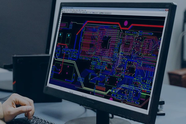
What is PCB Design and Layout
PCB design and layout is the process of creating the physical layout of a printed circuit board, which is used to connect electronic compo-nents in a circuit. The process involves designing the placement of electronic components, routing the electrical connections between them, and defining the shape and size of the board. MOKO Technology provides a full scale of printed circuit board design services, with a highly experienced design team that specializes in all kinds of printed circuit board design, from simple to complex.
Our PCB Design and Layout Services
- Schematic Design
Creating a graphical representation of an electronic circuit using standardized symbols and notations.
- PCB Layout Design
Placing components on the PCB, routing connections between them, and optimizing the layout for performance and manufacturability.
- Library Creation
Building and maintaining a library of parts and components that can be used in multiple PCB designs.
- Design for Manufacturability
Identifying potential issues in the design that may affect the manufacturability of the PCB, like component placement and trace widths.
- Prototype Assembly &Testing
Building and testing a prototype of the design to verify functionality and performance.
- Design Review & Optimization
Conducting a thorough review of the design to identify potential issues and areas for improvement.
PCB Design Capabilities
Comprehensive Design Capabilities:
• Mixed technology, Surface mount, through-hole designs
• Micro BGA/Micro Via/Blind and Buried Via
• Analog and Mixed Signal Design
• High-speed Digital Design
• RF design
• Sensitive analog circuits
• Reverse engineering
• Signal Integrity/Design Verification
• EMI inspection
• Compliance Engineering
…
PCB Design Software:
• Altium
• Mentor
• CADSoft (EAGLE)
• PADS • Cadence
• Allegro
…
Why Choose Us

Extensive Expertise
MOKO has extensive experience and expertise in PCB design and layout, and has completed many successful projects for a variety of clients in different industries.

High Quality
Our design and layout process adheres to industry standards and best practices, ensuring high-quality designs that meet or exceed customer expectations.

Full Support
We provide comprehensive support throughout the design and manufacturing process, including troubleshooting and resolving any issues that arise.

Quick Lead Time
We are committed to delivering reliable printed circuit board designs as fast as one day, helping customers to accelerate their time-to-market.
Our Proven Projects
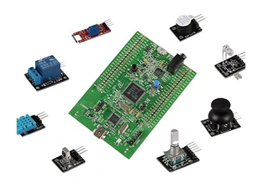
ESP32 + Lora Control Board
Customer Demand: ESP32 and LoRa technol-ogy energy monitoring,connect to custome-rs’cloud server
Our Support: Schematic design & circuit board design &embedded software design,SDK,Sam-ples,mass production,certification services.
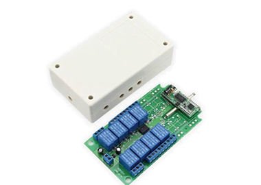
Smart Sensor PCBA Board
Customer Demand: STM32, printed circuit board design, CO2 & NH3 sensor, T&H sensor,ToF & GD sensor, IR sensor, pir motion detector light sensor, 3-axis accelerometer.
Our Support: Schematic design & printed circuit board design, embedded software design,mass production.
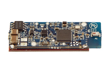
BLE 6-Axis Sensor PCBA
Customer Demand: CC2640, output voltage follows specific & realtime waveform,six-axis G-sensor.
Our Support: Schematic design & printed circuit board design, firmware, SDK enclosure design, mass production.
PCB Design and Layout FAQs
Some of the key steps are schematic capture, component placement, routing, design rule check (DRC), simulation and generating Gerber for manufacturing.
PCB design rules are a set of guidelines that specify trace width, spacing, size of the via and clearances to meet the electrical functionality, structural integrity and manufacturing standards.
Some of the widely used PCB design software are Altium Designer, Eagle, KiCad, OrCAD, Cadence Allegro, etc.
Component placement will affect the over efficiency and the durability of the circuit. Right placement leads to right placement of traces, miniaturization of the board size and improvement of signals and thermal integrity.
Simulation tools give details on the functionality of a circuit and could be used in detecting faults before the fabrication of the PCB. It can simulate almost all aspects of the circuit board for example signal integrity, power integrity, thermal integrity and many others.
They are: wrong placement of components, thin trace width, missing decoupling capacitor and inadequate spacing of traces.
When designing the PCB layout, certain matters may affect signal integrity of the board. They are trace routing, impedance control, grounds and/or planes as well as component placement which have led to the generation of noise, crosstalk, and reflections on signals.
We can design single-sided, double-sided, multi-layer PCBs, flexible circuits PCBs, and rigid-flex circuits PCBs.
Yes, we do provide PCB prototyping service to verify the design before mass production.
For simple designs, it only take 1-3 days; while for some complex designs, it may take 1-2 weeks.
We accept Gerber files, Bill of Materials (BOM) in various formats (.xlsx, .csv, .txt), Schematic files (.sch, .SchDoc, etc.), ODB++ data, and native files from major PCB design software.
Of course, yes. We do comprehensive DFM checks to ensure that the PCB design is optimized in respect to manufacturing to reduce possible issues and costs.
