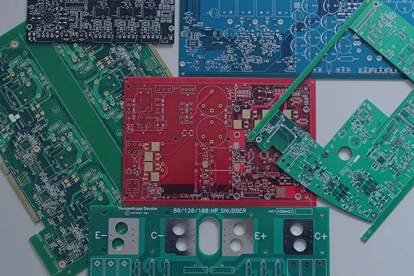
Multilayer PCB
MOKO Technology specializes in manufacturing kinds of multilayer PCB, from double-sided PCBs to 3-layer, 10-layer, and up to 50-layer PCBs.
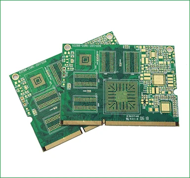
What Is Multilayer PCB
A Multilayer PCB (Printed Circuit Board) is a type of circuit board that has multiple layers of conductive material and insulation layers sandwiched together to form a complex circuitry design. MOKO Technology, as a leading PCB manufacturer in China, has extensive experience and expertise in multi-layer PCB fabrication. We provide custom-tailored solutions for customers in different industries to meet their specific needs, we can fabricate 3 layer PCB, 4 Layer PCB, 8 Layer PCB, 10 Layer PCB, 12 Layer PCB, 16 Layer PCB, 20 Layer PCB…
Why Choose MOKO

We have a stringent quality control process to ensure that each circuit board is inspected before delivery. We are certified with ISO9001, ISO13485, RoHS, UL, etc.

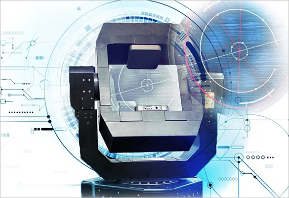
MOKO applies advanced fabrication technologies and machines to improve productivity efficiently, we can deliver multiple PCB with fast turnaround times.

Engaging in PCB manufacturing for nearly 20 years, we have all technologies and expertise required to manufacture high-quality PCBs.

Our in-house PCB manufacturing service enables us to better control costs and quality, providing customers with competitive prices.
Advantages of Multilayer PCB
- Increase Functionality: Multiple layers of boards allow us to fit more components and circuitry on the board, which can increase the functionality and capabilities of circuit boards efficiently.
- Reduced Size: The layered design of a multi-layer PCB is smaller than other PCBs with the same function, because the laminated layers can save a lot of board space.
- Lightweight: The layered configuration of multi-layer PCB can eliminate the need for connectors for separate PCBs, so as to reduce the overall weight of the board.
- High Durability: Multi-layer PCBs use multiple layers of insulation between circuit layers, bonding them together with adhesives and protective materials, which increases their durability.
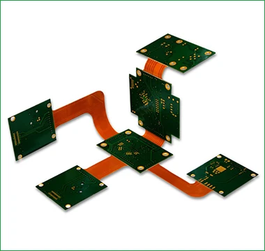
Application of Multilayer PCB


Multilayer PCB Capability Overview
Our Proven Projects
Multilayer PCB FAQs
A single-layer PCB has only one conductive layer while a multilayer PCB has more than two conductive layers, multiple layers stack together to achieve more functions and better performance.
Some of the benefits of using multilayer PCBs include: improved design flexibility, higher component density, enhanced signal quality, reduced EMI, and overall smaller board size.
Multilayer circuit board costs more than single-layer PCBs or double layer PCBs, which also has longer production time due to the complex circuit design.
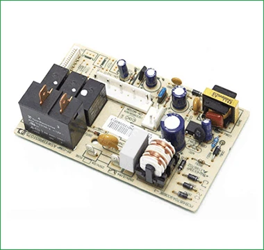
Multilayer PCBs are mostly applied in the telecommunication sector, aerospace industry, medical electronics, automobile technologies, and home appliances.
Compared to one or two layer PCBs, multilayer PCBs are relatively costly because of their manufacturing difficulty and increased material usage.
Challenges include managing signal integrity, layer alignment, thermal management, and increased design complexity, all of which require careful planning and expertise.
Yes, the multilayer PBCs are capable of handling higher power and temperature if they are designed with high thermal conductivity materials and proper heat dissipation techniques.
MOKO Technology can manufacture multilayer PCBs with up to 50 layers.
Yes, our engineers with the profound experience have the ability to give the right suggestion in designing your multilayer PCB to make it as per your performance requirement.
Yes, we conduct comprehensive testing services like AOI, ICT, and functional tests so as to increase reliability and quality.