High-Reliability
AI Server PCB Assembly
MOKO supports demanding AI server PCBA production with fine-pitch SMT, high ball-count BGA assembly, controlled reflow, testing, and reliability-focused process control.
Why AI Server PCB Assembly Is More Demanding
Compared with traditional electronics, AI server hardware has higher requirements for PCB assembly. Tight control is needed throughout the assembly process for high component density, complex IC packages, significant thermal loads and long operating hours.

Dense layouts increase the complexity of component placement, soldering, inspection, and rework.

Fine-pitch QFN, BGA, and FCBGA packages leave less margin for printing and placement variation.

BGA and FCBGA packages with dense ball arrays require precise process control and inspection of hidden solder joints.

High thermal loads and long operating hours place greater demands on solder-joint reliability.
Our AI Server PCB Assembly Capabilities
From complex package assembly to precision SMT process control, MOKO supports the demanding manufacturing requirements of AI server PCBAs.
Assembly Technologies: SMT, THT, Mixed PCBA assembly, BGA & FCBGA assembly
Component & Package Types: QFN, BGA, FCBGA, LBGA, Micro BGA, Fine-Pitch Packages
Solder Paste Printer Accuracy: ±0.03 mm
Component Placement Accuracy: ±0.03 mm
Minimum Pin Spacing: 0.20 mm
Production Capacity: 5 SMT Lines, 3 DIP Production Lines, Up to 1.2 Million pcs/day
Inspection Methods: AOI, X-ray inspection, and visual inspection for assembly and solder-joint quality verification
Testing Methods: Flying Probe, ICT, and Functional Testing
BGA Rework: BGA replacement and IR rework
Production Models: Full turnkey, partial turnkey, and consigned/kitted assembly
AI Server PCBA Manufacturing Process
During the AI server PCBA manufacturing process, each step is tightly controlled from material preparation and precision SMT assembly to reflow, inspection, and testing.
Featured AI Server PCB Assembly Project
High-Density AI Computing PCBA
An AI computing project demonstrating how MOKO overcame the challenge of micro-spacing soldering, high ball-count BGA assembly and long-term solder joint reliability with targeted process control.
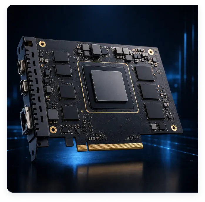
Product Key Features
14 Stress-Sensitive SMD ICs
10 devices on the TOP side and 4 on the BOT side.
0.20 mm Minimum Pin Spacing
Narrow pin-to-pin spacing created a demanding SMT process window with an increased risk of solder bridging.
QFN84 — Power Management
0.65 mm pitch · 84 pins · 16 × 16 mm
FCBGA1088 — MCU / MPU / SoC
0.65 mm pitch · 1,088 balls · 23 × 23 mm
LBGA196 — Memory
1.0 mm pitch · 196 balls · 15 × 15 mm
01
Micro-Spacing Soldering
The spacing between pins was as narrow as 0.20 mm, which increased the risk of solder bridging, so the SMT process needed to be tightly controlled.
02
High Ball-Count BGA Assembly
Both the FCBGA1088 and LBGA196 packages needed uniform solder paste application, precise component placement, and temperature control during reflow to ensure high quality of solder joints.
03
Long-Term Solder-Joint Reliability
The continuous operation at high temperature put stringent requirements on the reliability of the products. Thermal cycling, thermal shock, mechanical stress, creep and other factors had to be considered to reduce the risk of solder-joint failure.
PCB Surface Finish & Pad Optimization
The concentration of sodium hypophosphite, immersion gold reaction time and temperature were well-controlled during the ENIG process to minimize the risks of forming black-pad and brittle-joint. And the NSMD pad design was applied to reduce solder-joint stress concentration.
Precision Solder Paste Printing
A nano stencil and Senju Sn3.0Ag0.5Cu solder paste were used, with solder paste transfer efficiency controlled at ≥95% and squeegee hardness maintained at Shore D 80–90.
Precision Printing, Placement & Reflow
For this project, the accuracy of the printer was maintained within ±0.03 mm, the accuracy of the component placement within ±0.03 mm and the fluctuation of the transverse reflow temperature within ±1.5°C.
Solder-Joint Reliability Control
Reflow process parameters were tightly controlled to reduce the risks of Kirkendall voiding, irregular IMC formation, phosphorus enrichment, and Head-in-Pillow defects during double-sided BGA reflow.
Reliability Validation
Solder-joint fatigue testing and temperature cycling were used to evaluate solder-joint reliability under the project requirements.
≥99.8%
SMT First Pass Yield
≥99.6%
FCT First Pass Yield
The controlled process achieved stable, high-yield assembly for this high-density AI computing PCBA.
Why Choose MOKO for AI Server PCB Assembly
Beyond complex SMT assembly, MOKO provides integrated manufacturing support to help move your AI server PCBA from engineering preparation through production and quality verification.

Complex Assembly Expertise
Experience with fine-pitch QFN, high ball-count BGA/FCBGA, and high-density PCB assemblies for demanding computing hardware.

Precision Process Control
Tight control of solder paste printing, component placement, and reflow helps maintain consistent solder-joint quality in demanding assemblies.

PCB-to-PCBA Manufacturing
Integrated PCB fabrication and assembly support simplifies manufacturing coordination from bare PCB to finished PCBA.

Quality & Reliability Focus
Inspection, testing, and reliability-focused process control help address the stringent quality requirements of AI server PCBs.
AI Server PCB Assembly FAQs
AI server PCB assembly is the process of placing electronic components such as GPUs, CPUs, and HBM memory on a bare AI server PCB and soldering them together to create a functional PCBA.
An AI server PCB is the bare circuit board, and an AI server PCBA is the board with electronic components soldered and connected.
AI server PCBs usually feature high component density, complex IC packaging, and high ball-count BGAs. They also need to handle significant thermal loads and meet high reliability requirements. As a result, printing, placement, reflow, inspection, and testing must be controlled more strictly to meet these demands.
The cost is dependent on complexity of PCB, types of components, production volume, sourcing, inspection, testing, and reliability requirements.
Take into account component density, fine-pitch packages, BGA/FCBGA layout, thermal management, inspection and testing requirements.
Commonly used parts include processors, memory (DRAM, HBM), power management ICs, controllers and BGA/FCBGA packages.
Testing depends on the product and customer requirements and can include X-ray inspection, AOI, electrical testing, functional testing and project-specific reliability testing.
Yes. MOKO Technology has the capability to assemble AI server PCBs with high ball-count BGAs and fine-pitch FCBGA packages.
To get a quote, you usually need to provide the Gerber files, BOM, assembly drawings, pick-and-place data, testing requirements, and expected production quantity.
Start Your Project
Looking for a Reliable AI Server PCB Assembly Partner?
Whether your project involves high-density SMT, complex BGA packages, or demanding reliability requirements, MOKO helps bring your AI server PCBA from design to production.