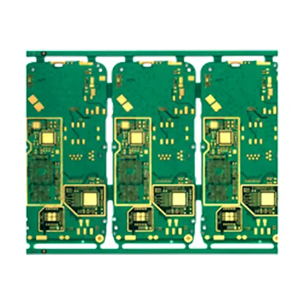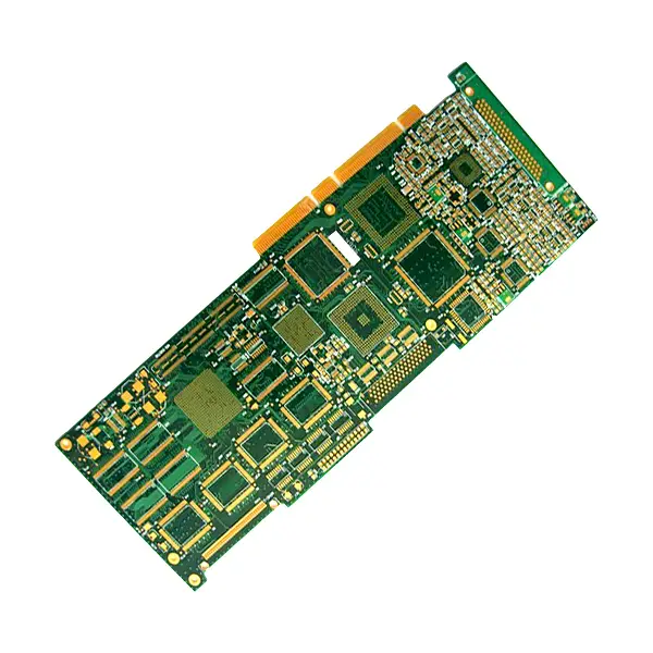

| Layer Counts | 2-16 layers |
| Base Material | FR-4, Rogers and Megtron laminates are optional |
| Board Thickness(mm) | 2.4mm |
| Max board size(mm) | 570*670mm |
| PCB size tolerance | ±0.2-0.3mm |
| Min. Hole Size | 0.1mm |
| Min. Line Width | 4mil |
| Copper Weight | 2oz |
| Surface Finish | ENIG, HASL, OSP are available |
| Certificate | UL, IPC-6012, RoHS, ISO 9001, ISO14001 |
Add a review
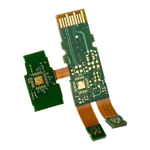
2-16 layer hdi multi-layer pcb
Your review
* Review is required
Name
* Name is required
Email
* Email is required
Add photos or video to your review
* Please tick the checkbox to proceed
* Please confirm that you are not a robot
| 5 star | 0% | |
| 4 star | 0% | |
| 3 star | 0% | |
| 2 star | 0% | |
| 1 star | 0% |
0 of 0 reviews
Sorry, no reviews match your current selections