
5G PCB Design: What Manufacturers Need to Know?
As 5G networks roll out globally, they promise to transform connectivity and push the boundaries of what’s possible with mobile technology. But to fully harness the potential of 5G, another

As 5G networks roll out globally, they promise to transform connectivity and push the boundaries of what’s possible with mobile technology. But to fully harness the potential of 5G, another

The copper traces on a printed circuit board carry electronic signals and distribute power between components and devices. This complex network of conductive pathways allows all the functional elements on the

Bluetooth is everywhere these days! You can find it in smartphones, headphones, speakers – pretty much any gadget that connects wirelessly likely uses Bluetooth. So when building a new electronic

PCB trace width specifically refers to the width of copper traces that carry vital signals and power across the printed circuit board. Determining appropriate trace widths is an important PCB design
The growing demand for advanced electronics drives innovations in circuit board capabilities and performance. Circuit designers now routinely work with faster signal speeds. High-speed signals, once an occasional challenge, are
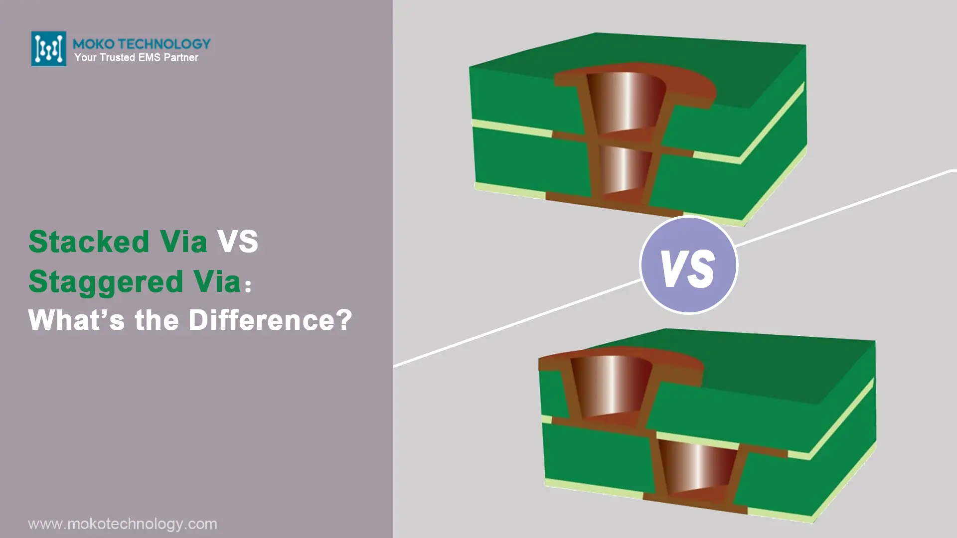
A common question when designing complex printed circuit boards for advanced electronics is whether to use stacked or staggered vias to route connections between layers. Vias act as conductive pathways
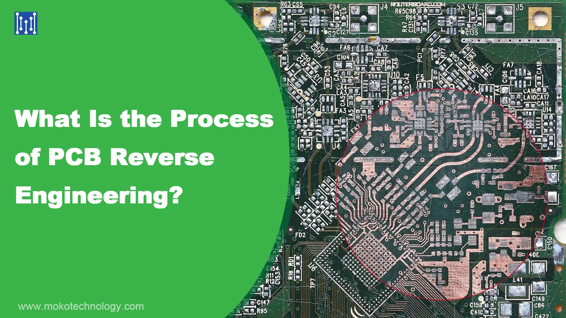
PCB reverse engineering refers to the process of analyzing and understanding the design, layout, and functionality of a printed circuit board by taking it apart, examining its components, tracing its
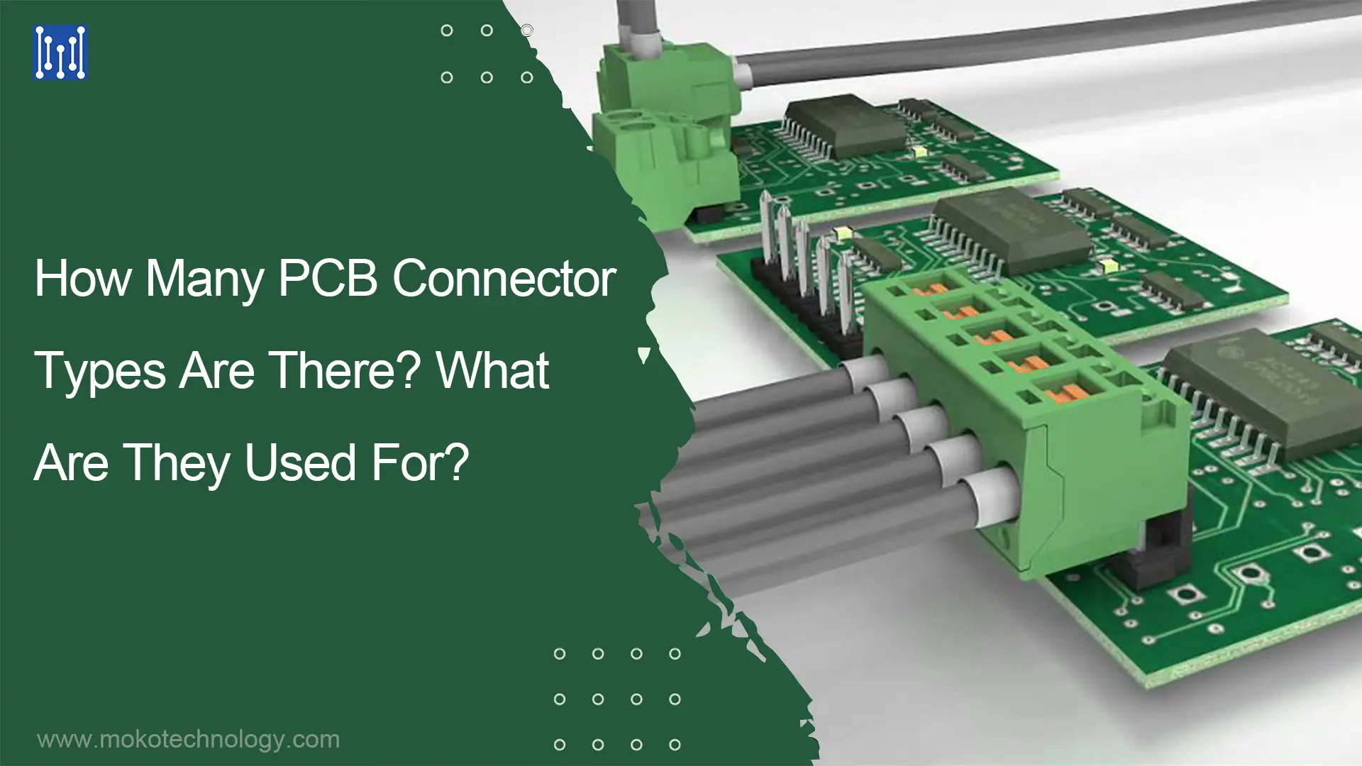
As electronic devices shrink but gain capabilities, efficient and durable interfaces become critical for connecting components within tight spaces. Circuit board connectors serve the essential role of linking the many
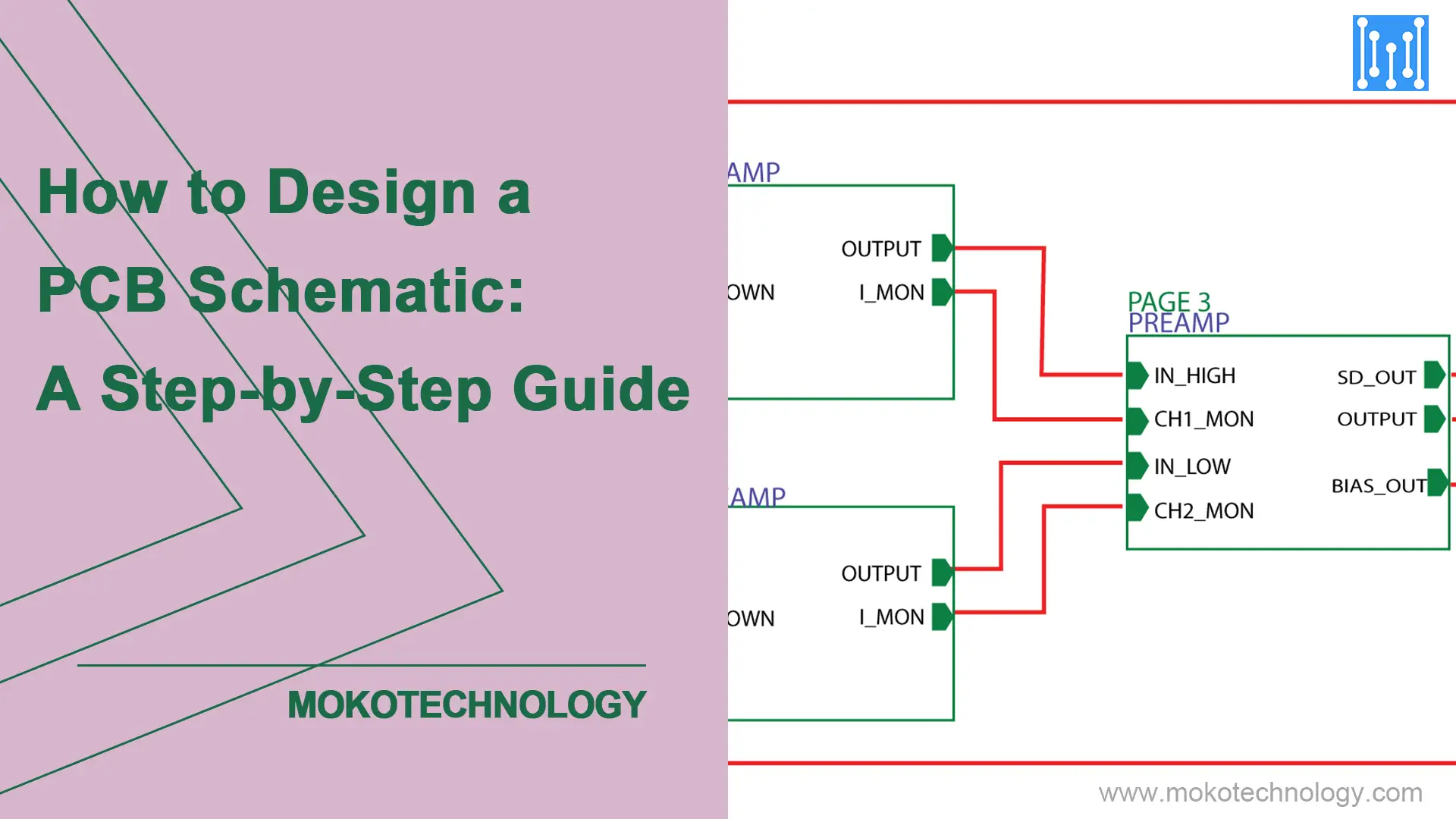
PCB Schematic: What Is It? Why Is It Important? A printed circuit board design starts with a PCB schematic diagram. This PCB schematic layout visually depicts the electronic circuit as a graph,