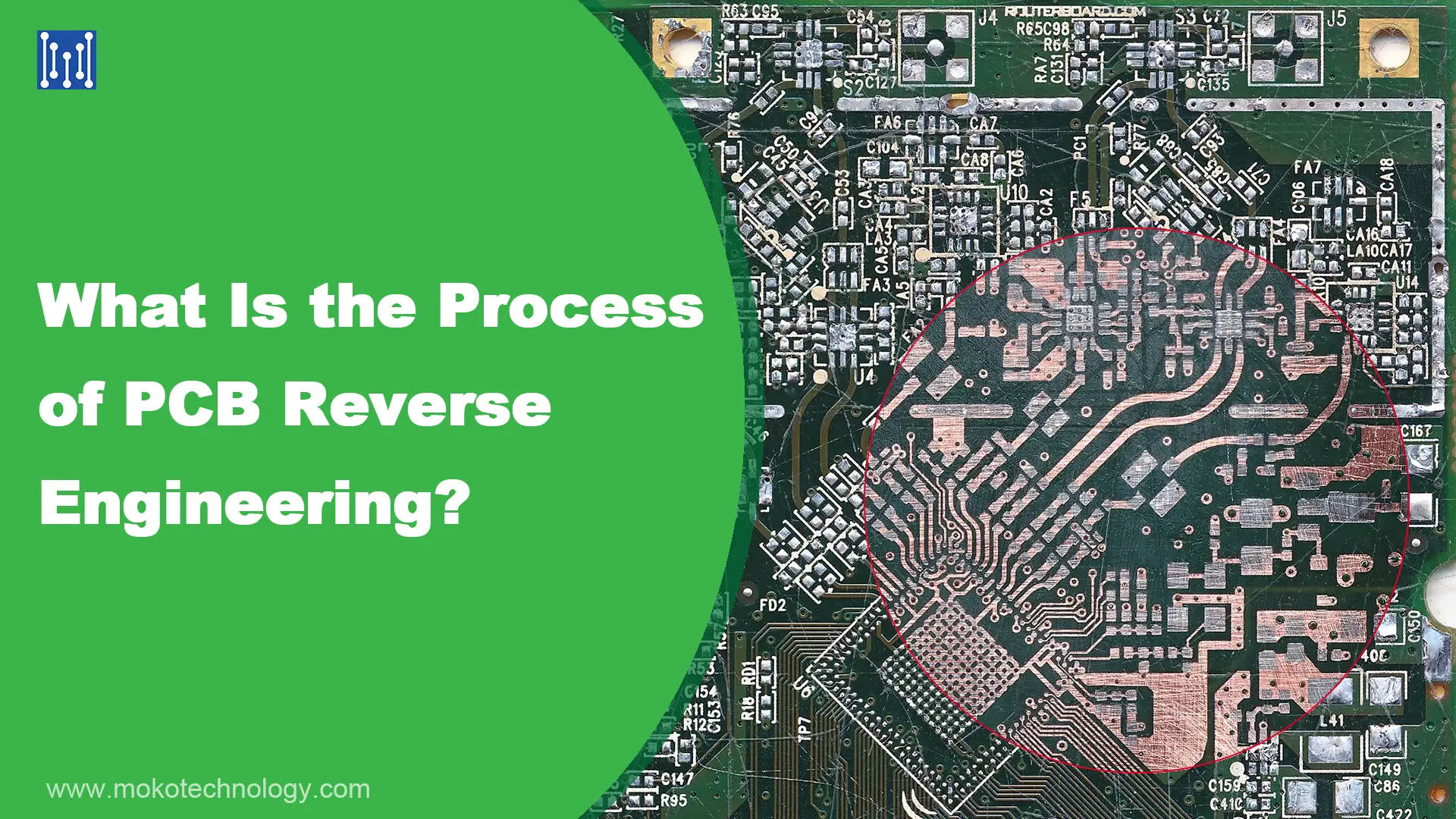
PCB reverse engineering refers to the process of analyzing and understanding the design, layout, and functionality of a printed circuit board by taking it apart, examining its components, tracing its connections, and creating a PCB schematic or layout diagram without having access to the original design documents or plans. PCB reverse engineering is often done for various reasons, including understanding how a competitor’s product works, recreating a discontinued or obsolete PCB for repair or modification, or assessing the security vulnerabilities of a device. In this blog post, we will provide an overview of the PCB reverse engineering process step by step so you can better understand it. Let’s dive right in.
The Process of PCB Reverse Engineering
Step 1:
Obtain the target PCB. Document layout by photographing and diagramming all component positions, orientations, and details on paper, especially diodes, transistors, and IC gaps. Take clear, well-lit photos of the full board for reference. As PCBs get more complex and miniaturized, tracing copper visually aids component identification.
Step 2:
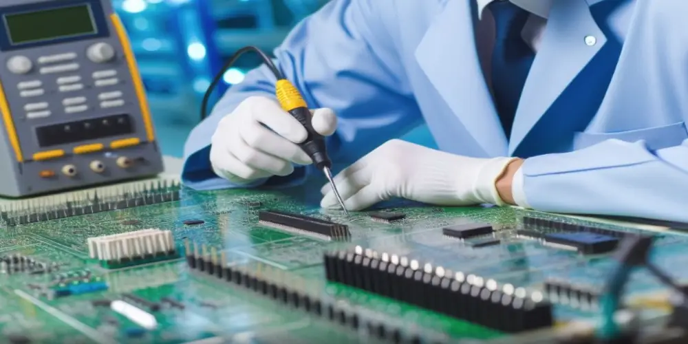
Remove all components by desoldering. Clean the board thoroughly with isopropyl alcohol removing all debris before scanning. Scan at 600+ dpi after gently polishing copper layers to make them shiny. Scan the top and bottom layers separately in high-resolution color, with the board completely flat to the scanning surface.
Step 3:
Import scans to Photoshop. Adjust levels until copper traces are highly visible and distinct from the substrate. Convert the bottom layer to black-and-white and review closely to ensure the scan captured all tracings sharply without disconnections. Save optimized layers as BMP files named “TOP” and “BOTTOM”. Use software to fix any trace defects evident in the scans.
Step 4:
Open BMP files in PCB design software. Convert to native format. Use alignment tools to overlay pad holes, vias, and matching points between layers precisely. Significant deviation indicates restart at an earlier stage is required for accuracy.
Step 5:
Start with the top layer scan. Trace out all visible design elements to recreate layer, matching component placements to earlier documentation photographs. Route connections following scans to replicate copper traces electrically. Delete the scan layer after finishing the vector trace. Repeat the process for the bottom scan layer, using connectivity tools to validate connections between layers. Add filled zones for any internal ground/power planes. For tight multi-layer boards, enable transparency display modes with alignment guides for matching vias between layers.
Step 6:
Print 1:1 top silkscreen and bottom layer films. Carefully overlay these onto the target PCB, backlit to check for perfectly matched alignment of all elements vs actual boards. Fix any errors by further trace modifications until full validation is achieved.
Step 7:
With form and function accurately captured and verified match to original, printed circuit board reverse engineering process completes. Further test populated boards built from the reconstructed data to benchmark for electrical parity and validation of true functional duplication.
Benefits of Printed Circuit Board Reverse Engineering
Allows for remanufacturing of obsolete PCBs – Reverse engineering can re-create discontinued PCBs that lack support from the original equipment manufacturer. This makes it possible to repair and continue using equipment that otherwise would be completely unusable.
Facilitates PCB repairs – By understanding the design and components of a PCB through reverse engineering, faults can more easily be diagnosed and components replaced to repair damaged boards.
Enables custom modifications or improvements – With the schematics and an understanding of a PCB’s design via printed circuit board reverse engineering, engineers can suggest and implement modifications like adding new features or enhancing performance.
Lowers costs of replication for small production runs – Reverse engineering allows cloned PCBs to be created without the high initial engineering and prototyping costs, making small scale production more affordable.
Provides insight for interoperability design – Printed circuit board reverse engineering can analyze the inner workings of competitors’ products which then influences improved interoperability design.
Facilitates technological progress – While respecting intellectual property rights, responsible reverse engineering allows close study of innovative designs, spreads know-how, and fuels further creativity.
MOKO Provides Reliable PCB Reverse Engineering Service
MOKO Technology has nearly 20 years of experience in the PCB industry, besides PCB design and assembly, we also provide reverse engineering services. With in-depth analysis, we recreate discontinued boards, clone existing ones lost to obsolescence, or upgrade units to modern standards.
It’s important to note that while reverse engineering can be legal under certain circumstances, it might infringe on intellectual property rights or breach contractual agreements in some cases. Therefore, it’s crucial to thoroughly assess and understand the legal ramifications associated with this process. Our process legally remanufactures your PCB while respecting intellectual property boundaries. Before commencing work, we thoroughly vet projects to guarantee no rights infringement. This allows us to provide fully functional replacements that can repair, replicate, or enhance the capacity of your outdated electronics. Contact our team to kickstart your custom project today.
