Have you ever see a circuit board that you can actually see through? That is a transparent PCB, which combines technology and design, letting light pass through the transparent material. This blog will discuss transparent PCBs, their materials, benefits and limitations, design principles, and exciting applications driving their popularity in modern electronics.
What Is a Transparent PCB?
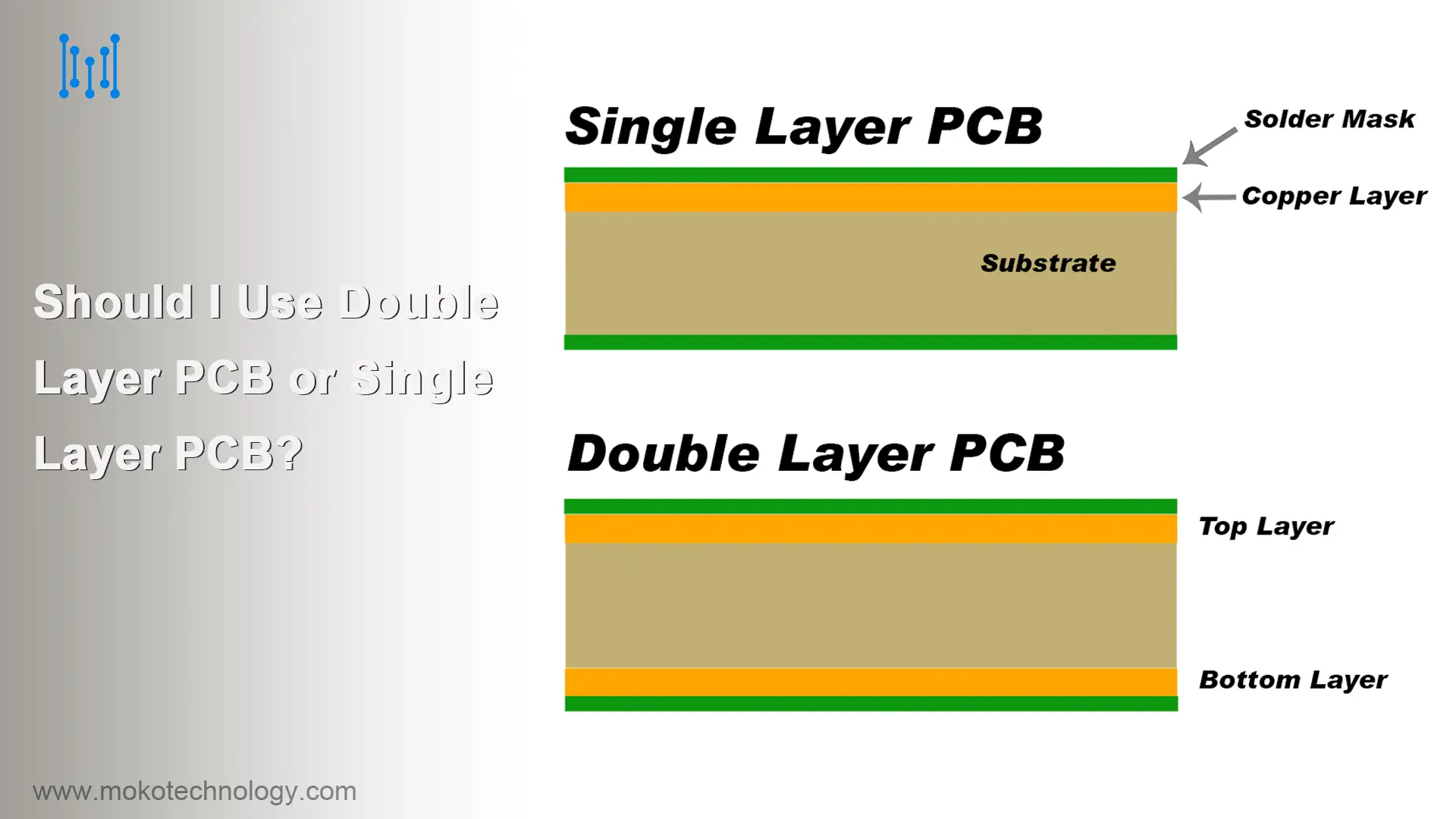
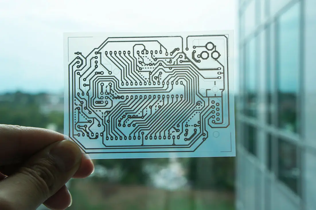
As the name implies, a transparent PCB(also known as clear PCB) is a kind of circuit board that enable the internal components and circuitry to be seen through from both sides of the board because it uses clear or semi-transparent materials as its substrate. While traditional PCBs normally use opaque materials as their substrate such as FR4 or some metal materials like copper, aluminum and so on.
Base Materials Used in Transparent Circuit Boards
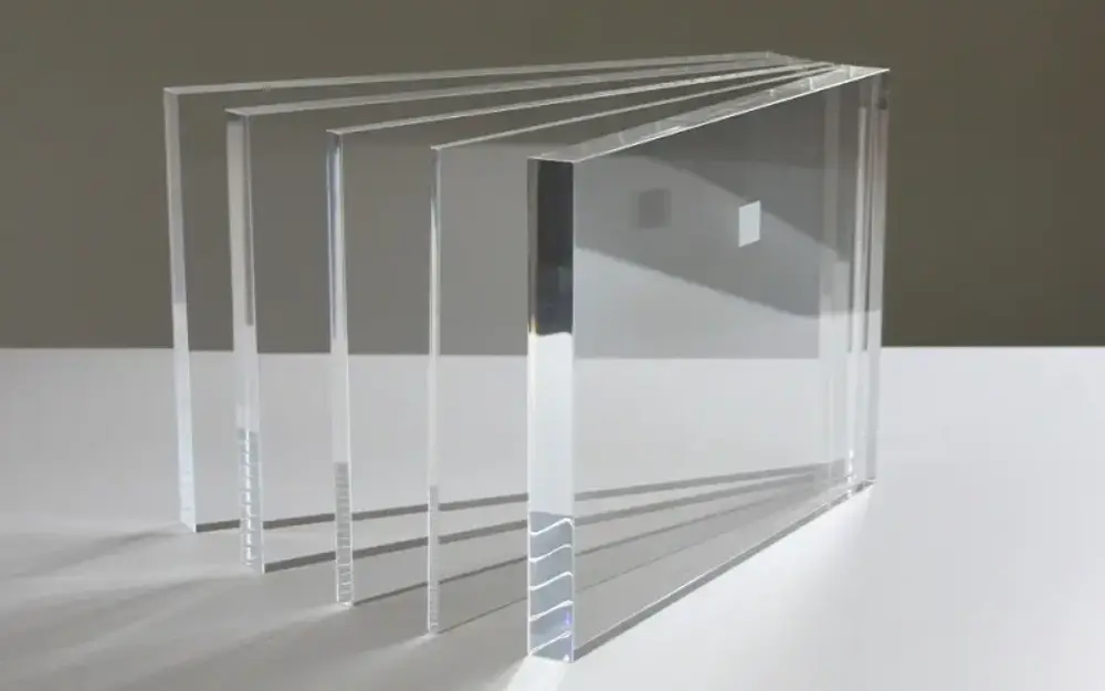
- Polycarbonate (PC): Polycarbonate is a clear, amorphous thermoplastic featuring great impact resistance, optical transparency, and high resistance to heat and chemicals.
- Polyethylene Terephthalate (PET): It is a crystalline polymer recognized for its toughness, heat resistance, and clear appearance.
- Polymethyl Methacrylate (PMMA): This transparent PCB material is also called acrylic or acrylic glass, which is an amorphous thermoplastic that has excellent light transmission and weather resistance.
- Glass-Reinforced Epoxy: This is a composite material consisting of glass fabric woven together with an epoxy resin, which is known to have remarkable dimensional stability, rigidity and is also optical transparency.
- Liquid Crystal Polymer (LCP): LCP is a high crystallinity thermoplastic that has a high chemical resistance and resilience to make very thin and flexible printed circuit boards (PCBs).
How Are Transparent PCBs Manufactured? (Step-by-Step Process)
A professional transparent PCB manufacturer follows these 10 precise steps to produce high-quality transparent circuit boards:
Step 1: Preparing the Substrate
Cut the transparent insulating base sheet to correct panel sizes, and then create openings for vias.
Step 2: Metal Layer Formation
Bond the copper foils to the transparent substrate by using optical-grade adhesive. This step is to create the conductive foundation for circuitry.
Step 3: Circuit Patterning
Coat a layer of photoresist onto the copper surface and transfer the desired circuit pattern onto the board through photolithography.
Step 4: Copper Etching
Use chemical etchants to remove unwanted copper areas, so as to keep the precise conductive pathways needed.
Step 5: Resist Removal and Hole Drilling
Strip off the remaining photoresist and then drill holes according to the circuit design.
Step 6: Copper Plating
Electroplate the through-hole walls and external layers of the board to ensure reliable electrical connections.
Step 7: Applying the Solder Mask
Apply a transparent, photo-imageable solder mask to the board to insulate the trace, but the soldering pads should be exposed.
Step 8: Legend Application
Print component symbols, labels, and alignment marks for easy identification with clear or semi-transparent inks.
Step 9: Board Routing
Each PCB is separated from the fabrication panel by precision cutting or routing.
Step 10: Quality Testing and Inspection
Finally, check the quality of each circuit board to ensure it meets the quality standards and performs as designed.
Advantages and Disadvantages of Transparent PCB
Benefits of Transparent PCB
- Easy troubleshooting: Thanks to its transparency, any issues in components, traces, or soldering can be detected easily by engineers without the need to disassemble the board.
- Lightweight and thin: Clear PCBs usually use base materials like PET, PMMA, or glass, which enable compact and lightweight circuit designs. Therefore, these boards are widely used in portable or aesthetic products.
- Excellent optical transmissivity: Transparent boards allow light to pass through efficiently, which is critical for LED applications.
- High heat resistance: Transparent printed circuit boards are highly heat-resistant. They can ensure stable performance even in high-temperature environments.
- Aesthetic appeal: Due to the transparent and modern appearance, these boards can appeal to more customers and create brand differentiation.
Limitations of Transparent PCB
- High manufacturing cost: Compared to traditional PCBs that usually use FR4 as the substrate material, transparent PCBs use more expensive base materials like PET and PMMA, which absolutely raise the manufacturing costs.
- Low fabrication yield: Fabricating clear boards require delicate materials and complex processing steps, which would lengthen the overall production time and reduce yield rate.
- Warping risk: For most transparent boards, their substrates are less rigid than traditional PCBs, making them more prone to deformation especially under stress.
- Laser drilling and hole limitations: As mentioned before, thin is an advantages of transparent PCBs. However, it can be a disadvantages as well. Thin board means a higher risk of cracking when applying laser drilling.
- Lower component density: To keep the transparency of the board, the board cannot be assembled with too many components or copper layers, which would limit the flexibility of the board design.
7 Design Rules for Transparent PCB
When designing transparent PCBs need to consider many factors such as electrical performance, manufacturability, and aesthetics. Follow the guidelines below help ensure reliable and efficient designs:
- Choose the substrate material according to the project budget and final use applications, considering parameters of the material like optical clarity, dielectric constant, and thermal resistance is necessary.
- Transparent PCBs have lower material resolution and higher resistivity than FR4 PCB, therefore, the trace width and spacing should be increased. Generally speaking, the minimum space is about 3–5 mils (75–125 µm) for most transparent materials.
- Keep the copper thickness within 1-2oz and design the board maximum 4 layers to keep the transparency. And the whole board thickness is 0.3–5 mm for flexible PET/LCP boards or up to 1 mm for glass substrates.
- Choose ENIG (Electroless Nickel Immersion Gold) or Immersion Silver finishes for good conductivity and smooth appearance.
- To maintain visual aesthetics, use transparent or reverse-mounted SMD components if it’s possible, and place the opaque parts in the correct positions to avoid blocking light paths.
- When designing transparent boards, conduct thermal simulations early to verify heat dissipation; For materials like glass and PET that have limited heat conduction, consider power plane distribution and decoupling capacitors for EMI control.
- Include alignment markers for precise pick-and-place and solder mask openings of at least 0.2 mm.
Applications of Clear PCBs in Modern Electronics
Key application areas of transparent PCBs include:
- LED lighting and displays: high-power LED modules, smart lighting, transparent display panels, etc.
- Consumer electronics: Smartphones, cameras, wearables, and foldable or flexible screens.
- Automotive systems: Tail lights, instrument clusters, and advanced braking systems (ABS).
- Medical devices: Imaging equipment, diagnostic devices, smart contact lenses and electronic skin.
- Industrial and automation equipment: Control panels, sensors, and compact system interfaces.
- Aerospace and defense: Utilized in optical sensors and infrared windows for aircraft and missiles.
- Architecture and interactive systems: Featured in illuminated panels, touch interfaces, and design installations for smart buildings.
Conclusion
Transparent PCBs are a symbol of modern electronics that incorporate functionality and beauty at the same time. Although they pose problems such as increased cost and complex production, their unique benefits such as better troubleshooting and exquisite looks among others are gradually earning them more value in various industries. With the further development of materials and fabrication methods, it can be expected that transparent PCBs will become more accessible, and more and more widely used in the areas of LED lighting, wearables, and automotive systems, among others.
FAQs
Q: Transparent PCB vs Traditional PCB: What’s the difference?
The main difference lies in the substrate material. Traditional PCBs use opaque materials like FR-4 fiberglass, while transparent PCBs are made from clear materials such as glass, PET, or PMMA that allow light to pass through.
Q: Is the price of a transparent PCB higher than that of a traditional PCB?
Yes. Transparent PCBs are generally more expensive due to the higher cost of clear substrate materials and the specialized fabrication processes required.
Q: What Is a flexible transparent PCB?
A flexible transparent PCB combines optical clarity with mechanical flexibility. It’s typically made from transparent polymers such as PET or LCP, allowing the circuit to bend or conform to curved surfaces while remaining see-through.