PCB pads are an important part of PCB manufacturing as they determine where the components will be soldered to the printed circuit board. If not done correctly, they can result in poor joints, short circuits, and assembly issues. No matter if you are creating your first board or optimizing an existing design, it is very important to know the PCB pad types and sizing standards to ensure successful PCBA manufacturing.
What Are PCB Pads?
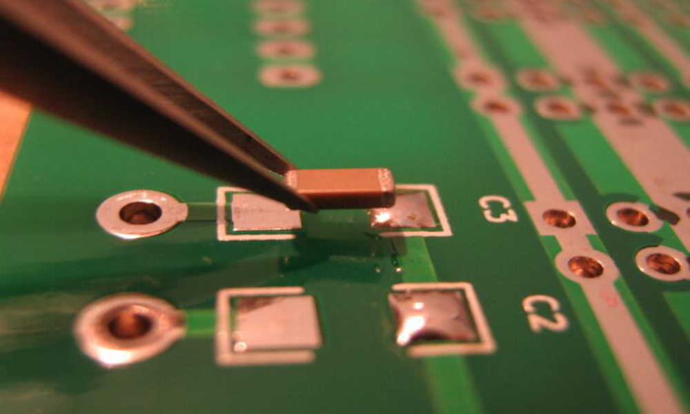
PCB pads, also known as soldering pads or solder pads, are areas on a printed circuit board that are specifically designed for the attachment of electronic components. These pads are usually shaped in round or rectangular forms, and made of copper or other conductive materials. PCB pads are used to connect the electronic components with the traces of the PCB. Typically, the solder pads are found at the ends of the traces where components are supposed to be placed. The design and placement of pads can directly affect the solderability, reliability, and thermal conductibility of the component.
Types of PCB Pads
PCB pads can be categorized into two main types based on the components and packaging methods: through-hole pads and surface mount pads.
Through-hole Pad
Through-hole pads are utilized for mounting through-hole components on a circuit board. These pads feature via holes where the pins of the components are inserted during the PCB soldering process. By soldering components via through-hole pads, durable solder joints are established, ensuring a dependable long-term mechanical and electrical connection to the PCB. However, it’s important to note that due to the presence of component leads and the necessary holes, the availability of routing space on a multilayer PCB may be restricted.
Through-hole pads can be divided into two types:
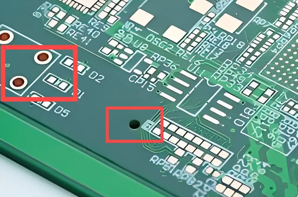
- Plated Through Hole (PTH) pads:
Plated Through Hole (PTH) pads are holes on a PCB with a thin layer of metal coated inside the hole walls through a plating process. This process creates an electrical path that connects different layers of the board, while also providing a secure mounting point for through-hole component pins.
- Non-Plated Through Hole (NPTH) pads:
Non-Plated Through Hole (NPTH) pads mean the hole wall has no metal plating. They are usually used in single-sided boards or for mechanical purposes, such as mounting the PCB inside a case or enclosure with screws or standoffs.
Surface Mount Pad
The surface mount pads are the pads that are used for attaching electronic components directly to the surface of the circuit board. The difference between through-hole pads and surface mount pads is that surface mount pads are used for mounting smaller components. These allow a greater density of components to be installed in a smaller area of the board. However, surface mount pads do not work for components that heat up a lot. The small packaging size of SMT can make it difficult to dissipate heat, causing overheating problems.
BGA Pads
BGA (Ball Grid Array) Pads belong to the category of surface mount pads, which are typically smaller and more densely packed than pads used for other surface mount components. And two types of BGA pads are commonly used:
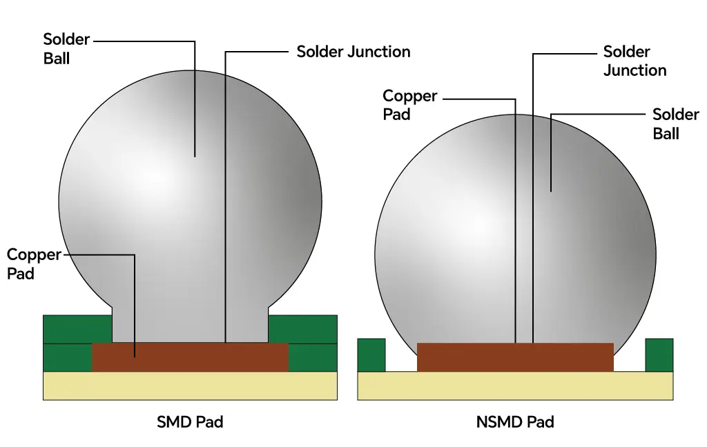
- Solder Mask Defined Pads (SMD)
SMD pads for BGA components are designed with solder mask apertures that are smaller than the diameter of the pads they cover. This is intended to minimize the size of the pad that the component will be soldered to. By applying the solder mask to cover a portion of the copper pad underneath, two advantages are achieved: Firstly, it helps secure the pads to the circuit board, preventing them from lifting off due to mechanical or thermal stress. Secondly, the openings in the mask provide a guide for each ball on the BGA to align with during the soldering.
- Non-Solder Mask Defined Pads (NSMD)
Non-Solder Mask Defined (NSMD) pads are a type of copper pad used in printed circuit boards that are not covered by the solder mask. They are often smaller in size compared to the diameter of the solder ball, typically reducing the pad size by around 20% of the ball diameter. This reduction in pad size allows for closer spacing between pads, enabling more efficient routing and making them suitable for high-density and fine-pitch BGA chips. However, NSMD pads have a higher susceptibility to delamination, which can occur due to thermal and mechanical stresses.
How to Determine PCB Pad Size and Dimensions
When designing solder pads, how do you determine their sizes and dimensions? Here are several reliable sources:
- Industry Standards
IPC-7351 is a widely adopted industry standard that defines surface mount land pattern specifications. Following this standard is a workable method for defining pad sizes.
- EDA Pad and Footprint Generators
Most modern EDA tools have built-in footprint generators. These tools help to calculate the correct pad size and dimensions automatically according to the selected components.
- Component Manufacturer Datasheets
Component datasheets will list a recommended PCB land pattern and the exact dimensions of the pads, which are regarded as one of the most reliable sources for engineers
- Online Pad Calculators
There are many free online pad calculators available, which enable engineers to verify pad dimensions easily without the need to open a full EDA tool.
PCB Pad Design Guidelines
When designing PCB pads, following these important guidelines can ensure reliable soldering performance and manufacturability.
Pad Size:
The size, shape, and spacing of the pads depend on the specific requirements of the components being used. Different types of components may have different pad configurations.
- For single-sided pads, the diameter or minimum width is 1.6mm
- For double-sided weak-line pads, it is only necessary to increase the aperture by 0.5mm, as too large a pad size will easily cause continuous welding
- For pads with apertures larger than 1.2mm or pad diameters larger than 3.0mm, consider designing them as special-shaped pads
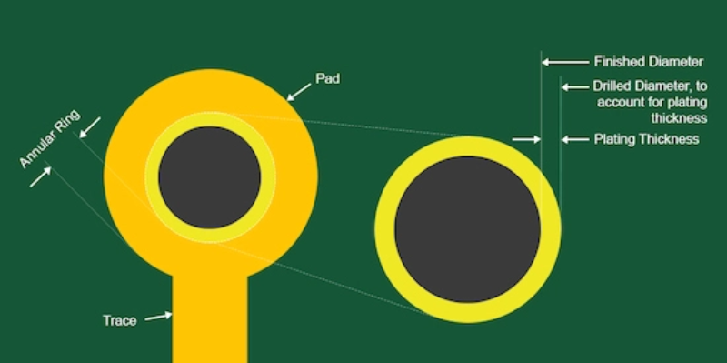
- The inner hole of the pad should generally not be less than 0.6mm, because the hole smaller than 0.6mm is not easy to operate when punching
Pad Spacing:
As to the spacing of pads, it is important to consider the size of the component pins that will be inserted or attached to the pads, while also taking into account the related component package. Different components have varying requirements for the spacing of the pad mounting holes.
- For axial components with pin diameters less than 0.8mm, the installation hole pitch is typically 4mm longer than the standard hole pitch
- If thepin diameter of an axial component exceeds 0.8mm, the installation hole pitch is generally more than 6mm longer than the standard hole pitch of the component body.
- Forradial components, the mounting hole spacing should match the spacing between the component pins.
Pad Clearance:
The edge-to-edge clearance between adjacent pads should be greater than 0.4mm to reduce the risk of solder bridging during assembly.
Conclusion
Selecting the right pad type, size, and spacing of PCB pads is not only a rule-based decision. These decisions directly influence the quality of soldering of your components, as well as the strength of the joints. They improve efficiency and reduce expenses in the long run, regardless of whether you are using surface-mount pads, through-hole, or BGAs pads. If you want to produc a high-quality PCBA , you need a good PCBA company to guarantee that your PCB has quality pads and reliable solder joints. With 20 years of experience, MOKO Technology provides a full range of one-stop manufacturing solutions, including PCB design, manufacturing, prototyping, component procurement, PCB assembly, and testing. Contact us today to get more details!
FAQs about PCB Pads
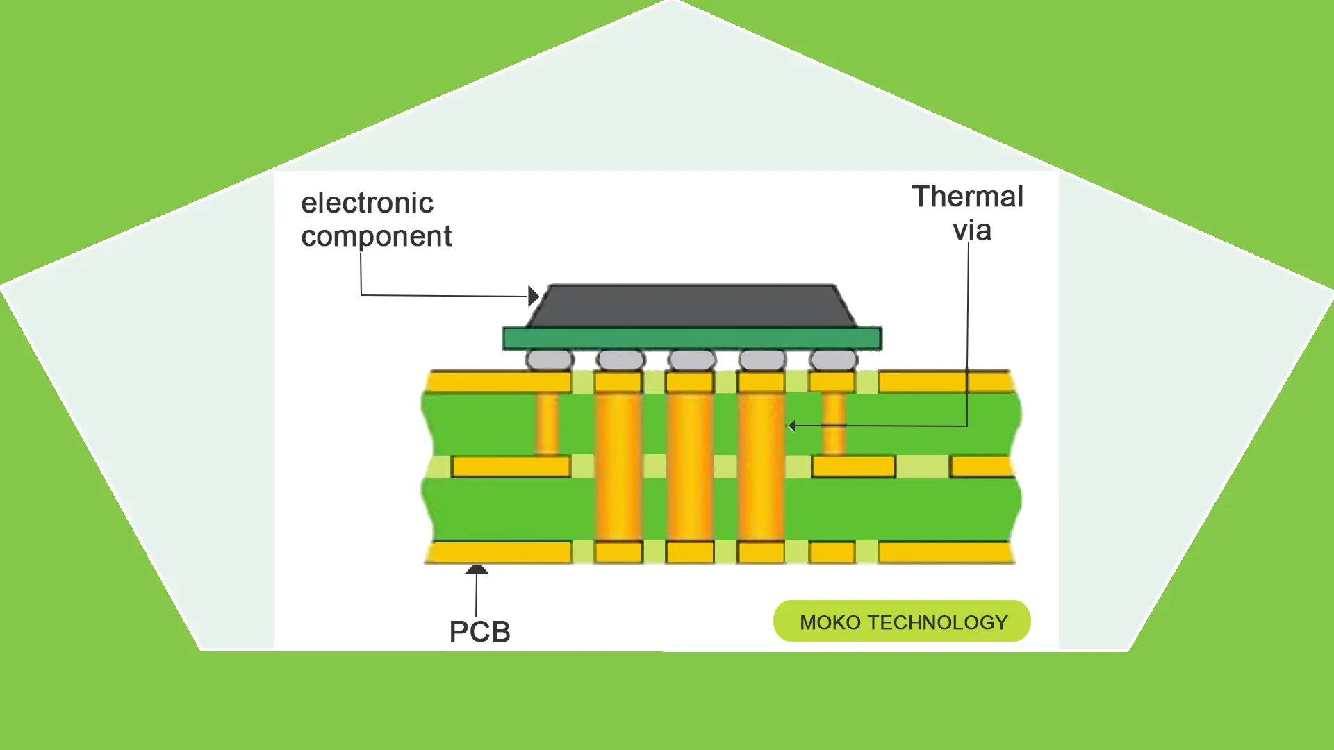
1. What is the difference between a PCB pad and a via?
PCB pad refers to the area of copper where component will be soldered to the board. The via is a hole that is plated and provides an electrical connection between layers of a PCB.
2. Can you put a via on a pad?
Yes, it’s called via-in-pad design, and it’s quite prevalent in components that have limited space, like BGAs and QFNs. The via is embedded directly into the pad and must be filled/plated to make sure that the solder will not wick down through the via during the assembly process.
3. What material are solder pads made of?
Typically, the solder pads are made of copper, which can offer excellent electrical conductivity. The copper surfaces are normally coated with coatings like HASL, ENIG or OSP to avoid oxidation and enhance solderability.
4. What is the difference between SMD and through-hole pads?
SMD pads are located on the surface of the board and are used for smaller components soldered directly onto the PCB. Through-hole pads feature a hole that goes through the board and are used for component leads that are soldered in place.