With the development of electronics integration, via in pad gradually became a frequent-used solution to handle limited space for several circuit paths. This text will deeply dive into what it is and how it is applied in design and manufacturing.
What Is A Via-in-pad?
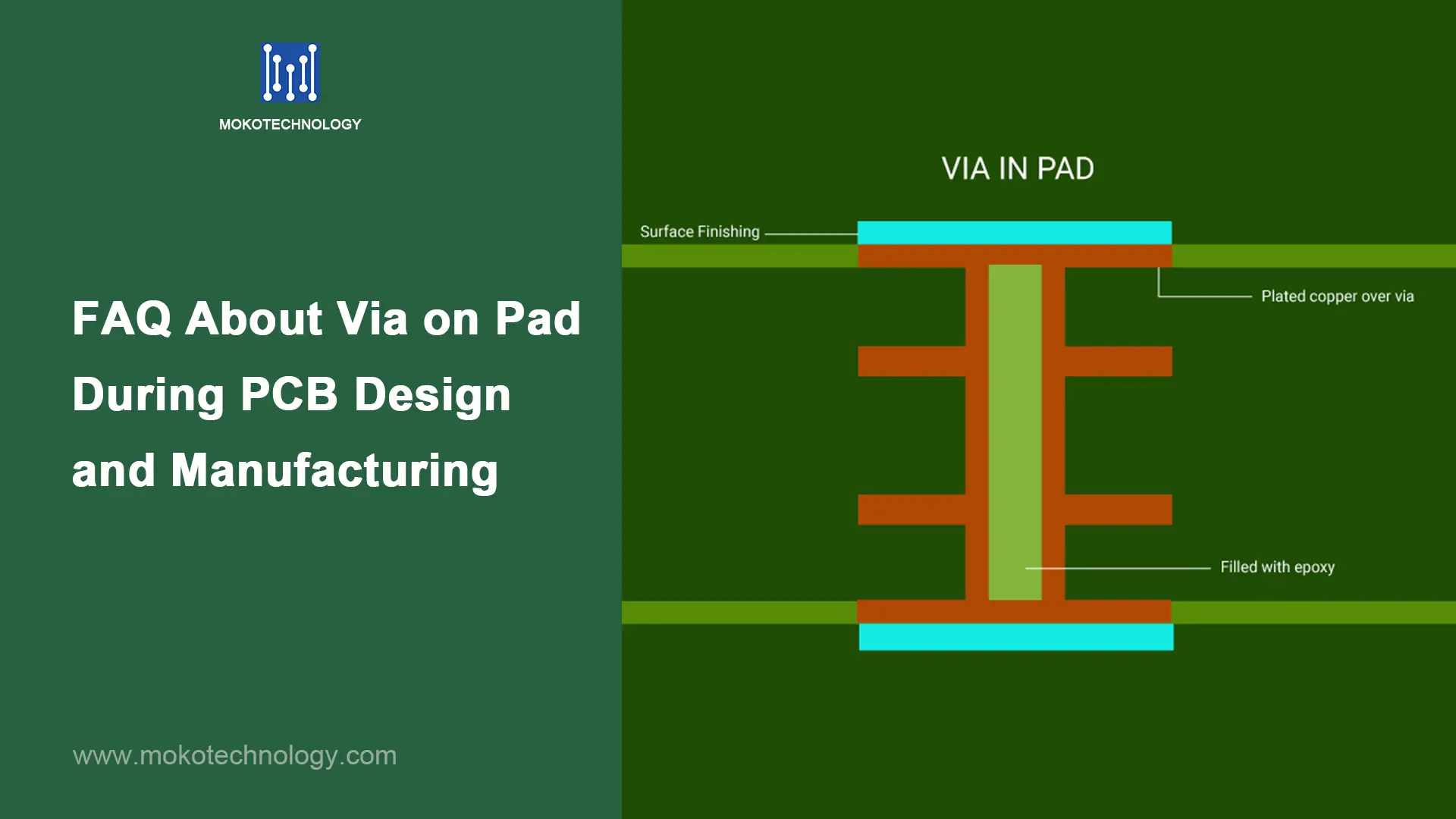
It refers to through holes drilled on the bonding pad, which is usually SMD type and BGA type above 0603 size. It goes through the whole PCB and is used for connecting different circuits on different layers. In common, it is always wrapped by copper which can conduct electricity.
What Are the Advantages of Via-in-pad Routing?
The most significant advantage of via-in-pad is fitting the circuit in a small board so as to realize more usefulness at low space cost. It simplified the circuit layout of BGA with short ball distance. Moreover, it makes the short distance between the electric capacity and the module possible by reducing layout on the surface of PCB. This greatly reduces electrical inductance. Last, the layout including via in pad makes ground attachment of high-frequency components easier.
What Are the Limitations?
Each coin has two sides. Via in pad brings about protrusion of PCB surface, so it needs extra effort and cost to remove this problem. And, more manufacturing steps are required. For example, we have to drill holes, plated the whole with conducting materials, fill the holes with epoxy resin, and cover them with copper. This process may also lead to new problems, such as air expansion while covering the holes, and void solder joints due to the release air.
Although limitations exist, via-in-pad is still a progressive technique against conventional via.
Conventional Via Vs. Via-in-pad PCB Design
The circuit path between conventional via and pins is just presented on the surface of the PCB, taking up lots of space. In contrast, via in pad leaves more space for building circuit paths. For example, tiny BGA with lots of pin is allowed to link not only to the PCB surface but also the pad inside via which go through all the layer of the PCB.
When to Use Via-in-pad in Design?
In addition to tiny BGA with so many pins, there are other situation where we can use it in design. For example, we highly recommend to use via in pad for GND pad under QFN package, which needs cooling heavily. And when you want to put filter capacitor on the back of BGA, you can use it under filter capacitor to avoid stepping on the through hole of BGA pins.
How to Use It for PCB Design and Manufacturing
When drawing it, there is something we need to notice. First, try to put all the tiny holes on the same layer of PCB. Second, ensure your solder mask cover the PCB surface side. Third, you should also consider the superb state of your PCB design for easy producing.
| Minimum | Maximum | |
| Via diameter | 0.20mm | 0.75mm |
| Board thickness | 0.40mm | 0.35mm |
| Thickness:diameter | / | 8 |
| Via distance | 0.20mm | / |
| Range value of via diameter | 0mm | 0.3mm |
| Distance between via and component holes | 0.25mm | / |
(Recommended PCB status to use via in pad)
It is not a difficult operate for most PCB designer, but things become complex when the drawing goes to manufacturing line. There are totally three manufacturing technique of via on pad.
- Common Via in Pad: Drill a through hole on the bonding pad. There is no specify operation during PCB manufacturing. Be careful of oversize holes which leads to tin leakage, since it may cause void soldering joint.
- Via in pad filled with epoxy resin: This is more complex in manufacturing line. First, fill the hole with epoxy resin. Then, cover the via by plated copper. The PCB surface will look so flat. Meanwhile, there will be no risk at tin leakage and void soldering joint.
- Via in pad filled with copper: This via is special for rapid heat conduction.
How to Fill Via in Pad PCB?
| Filling | → | Solidification | → | Polish | → | Reduce copper | → | Remove extra filler |
(the whole filling process for via in pad)
Although the wall of via is plated by copper, filling is necessary. Using scraping knife and vacuum draw machine, we can apply the liquid to the through hole. If the filler is epoxy resin, you should be careful about the flatness of PCB surface. Your PCB factory must offer solution to you if you contact them.
Via in Pad Application
It is widely used in high density PCB, such as smart phone integrated circuit board, telecom PCB, automotive PCB, medical device PCB and even IT PCB. We feel hopeful to the abroad application to it in the future, since we always love smaller PCB, closer components distance, and more PCB function.