Before you start designing your PCB, you need to decide whether you will use a double-layer or a single-layer PCB. We widely use both of these in everyday electronic devices. The kind of PCB you use primarily depends on what you are using it for. For intricate devices, it is recommended to opt for double-layer PCBs, while single-layer PCBs are more suitable for comparatively simpler devices. In this blog, we will list the advantages and limitations of each type of PCB, and explain how to choose between them according to your requirements. Let’s dive right in.
What Is Single Layer PCB?
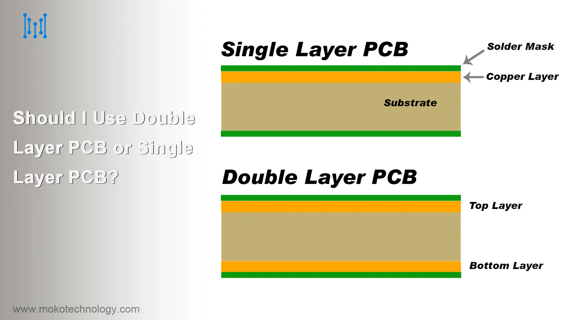
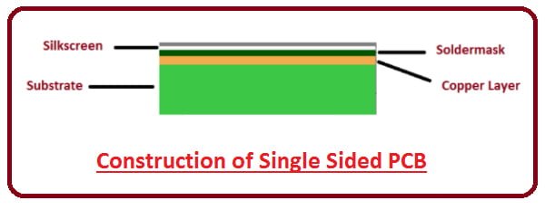
Single layer PCBs have a conductor material on one side and the components are placed on the other side. These boards have only one layer of conductive material which is mostly copper. A single layer board has a conductive material, a substrate layer, a protective solder mask, and then the silkscreen. We mostly use these boards in simple electronic devices.
Single-layer PCBs find their niche in various domains, thanks to their simplicity and cost-effectiveness. These boards are often utilized in low-cost electronics, prototyping, and DIY projects. Their ease of fabrication and affordability make them ideal for basic electronic devices, such as calculators, remote controls, and simple consumer electronics. Single-layer PCBs also serve as excellent platforms for educational projects and hobbyist ventures, where individuals can experiment with circuit designs and gain hands-on experience
What Is Double-layer PCB?
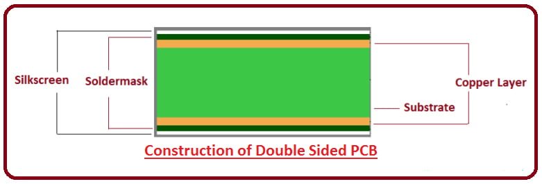
Double-layer printed circuit boards have one substrate layer like the single-layer boards. However, double-layer boards have two layers of conductive metal, one on each side. This configuration allows for the placement of electronic components and the routing of traces on both sides, thereby increasing the board’s density and functionality.
Double-layer PCBs excel in scenarios where more sophisticated circuit designs and higher component densities are necessary. These boards accommodate a larger number of components within a more compact space, making them ideal for applications such as telecommunications, automotive electronics, industrial control systems, and consumer electronics. Double-layer PCBs provide improved signal integrity and noise reduction capabilities, making them suitable for high-speed circuitry and applications that demand reliable performance. They are commonly employed in advanced electronics, including medical devices, aerospace equipment, and complex electronic systems, where precision, reliability, and miniaturization are critical factors.
Pros and Cons of Single Layer and the Double-Layer PCBs
Pros and cons of Single Layer PCBs
There are several advantages of single layer circuit boards, they are:
- Lower Cost
Single-layer PCBs provide a considerable cost benefit in comparison to double-layer PCBs. Their simpler design requires fewer manufacturing resources, resulting in lower production costs.
- Simpler Design and Production
Single layer PCBs are simple to design and produce in comparison to the double-layer PCB. And there is no need to use specialized equipment and skilled labor.
- Mass Production Techniques
Single-layer PCBs are often produced using mass production techniques such as panelization. Panelization involves placing multiple single-layer PCBs on a single larger panel, allowing for simultaneous fabrication and efficient use of materials. This technique enhances production efficiency and scalability, making it suitable for high-volume manufacturing.
- Short Lead Time
Single-layer boards have an easy manufacturing process, which contributes to a relatively short lead time. This makes them an ideal choice when there is an urgent need for PCBs in large quantities.
And their limitations include:
- Simplistic Design
The simplistic design of single-layer PCBs is their substantial limitation. A single-layer PCB won’t suffice when we need to make complex devices. The devices will not function properly if the wires cross each other. Hence, the board should have sufficient room for accommodating everything.
- Slower Speed and Low Capacity
The speed and power of these boards are also affected by their limited number of connections. They have a low operating capacity and therefore they don’t have enough power for certain applications.
- Lack of Component Density
Single-layer PCBs may struggle to accommodate a large number of components. This can be a limitation when designing complex electronic circuits that require numerous components.
- Routing Challenges
With only one conductive layer, routing traces can be more challenging. Components and traces must be carefully arranged and connected to avoid crossing or overlapping traces, which may result in longer trace lengths and increased resistance.
Pros and cons of Double-layer PCBs
Here we list the pros of double layer PCBs one by one:
- Increased Durability
Double-layer PCBs exhibit increased durability as a result of their additional layers, leading to a thicker structure compared to single-layer PCBs. This heightened durability enables the PCBs to withstand rough conditions and extends their overall lifespan.
- Useful for More Complicated Projects
Complex devices that involve more components often need a double-layer PCB. The double layers ensure that you have sufficient space for placing more components and connecting them.
- Smaller Size and Lighter Weight
Stacking layers on top of each other allows for a higher component density in a more compact space. Consequently, this compact design results in a reduction in overall weight.
Also, these boards have cons including:
- Higher Costs
It is more expensive to use double-layer boards and it requires more resources. On top of that, we need skilled labor and sophisticated equipment.
- Complicated Designing and Manufacturing
It is more complicated to design and manufacture double-layer boards. So, if you lack the resources then you might face many problems throughout the manufacturing process.
- Longer Lead Times
Since double-layer boards are more complicated therefore they have a longer turnover time. If you make a mistake during the manufacturing process or if there is a flaw in the design then it will be very difficult to rework. Also, it will increase the overall cost.
- Complex Repairs
Double-layer PCBs are very reliable, however, if they get damaged then it is very difficult to repair them. This is because of their complex design. A large number of components and their connections make it very difficult to identify and fix the problem.
Deciding Between Single-Layer or Double-Layer PCBs
To make an informed decision between single-layer and double-layer PCBs, it is essential to carefully assess your specific requirements and determine which type of PCB is better suited to meet them. You may do so by asking yourself these five questions:
What level of functionality would I need?
You should go with double-layer PCBs if you need them for complex applications.
What is the maximum size the board can be?
Double-layer boards have a smaller size and they have improved performance.
Is durability a major priority?
You should go with double-layer PCBs if the answer is Yes.
What is my budget?
If you have a modest budget, then single-layer PCBs are the best choice.
How quickly do I need the PCBs?
Single-layer PCBs have a shorter turnover time in comparison to double-layer PCBs.
MOKO Technology is a renowned name in the PCB industry, providing one-stop PCB manufacturing and PCB assembly services. We have a large manufacturing setup and we have mass production capacity. We have expertise in the production of both single-layer and double-layer PCBs. More importantly, we assist customers in selecting the most suitable PCB type for their projects. Contact us to kick off your PCB project now!