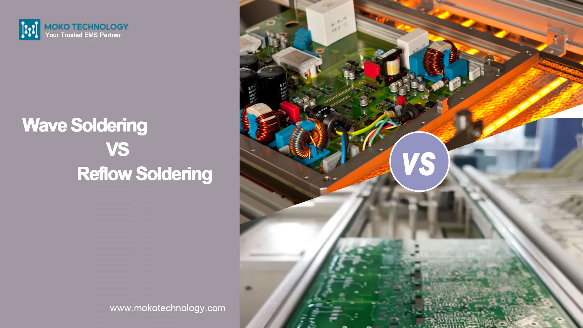
Soldering is an indispensable step in the PCB assembly process, which attaches the components to the circuit boards firmly. There are two popular methods of soldering used in the PCB industry: wave soldering and reflow soldering. They serve the same purpose but have different applications and operational principles. Understanding their differences and which type of soldering to use in different scenarios is critical. In this blog, we will compare these two methods, discuss their pros and cons, and help you choose the right process for your PCB assembly needs.
Wave Soldering vs Reflow Soldering: Key Differences at a Glance
Below is a brief comparison of these two approaches before going into the details:
| Aspect | Wave Soldering | Reflow Soldering |
| Component Type | Mainly THT components | SMT components (with selective THT) |
| Heating Method | Molten solder wave contacts PCB underside | Controlled heating curve inside reflow oven |
| Precision | Lower; suitable for larger leads | Higher precision; ideal for fine-pitch SMT |
| Production Volume | Very efficient for large THT batches | Excellent for high-volume SMT |
| Double-Sided Use | Limited (mainly single-sided) | Widely used; ideal for double-sided SMT |
| Equipment Cost | Lower | Higher |
| Ideal Applications | Power boards, connectors, simple assemblies | High-density consumer electronics, IoT, telecom |
Now that we have understood the main differences in wave soldering vs reflow soldering, let’s take a closer look at how each process operates. We will start with wave soldering.
What Is Wave Soldering?
Wave soldering attaches components to a circuit board using a wave of molten solder. As the board passes over the wave, the solder flows underneath and coats the component leads to create secure connections. This method is especially efficient for mass-producing boards with through-hole components.
The Wave Soldering Process
Wave soldering involves 4 steps and we will look at them one by one.

1. Flux spraying
The first step is to apply the flux to the components that need to be soldered. The major functions of flux are to remove surface oxides and prevent oxidation during the soldering process, which helps the solder bond properly to the metal.
2. Pre-heating
PCBs travel through a heat tunnel in a pallet along a chain which is similar to a conveyor belt. It is necessary for activating the flux and carrying out pre-heating.
3. Wave soldering
When the temperature continues to rise, solder paste melts to become liquid. This results in a wave of solder which travels throughout the board and allows components to solidly bond with the board.
4. Cooling
The wave soldering profile is conformed to the temperature curve. The curve starts to plummet after the temperature reaches its peak in the wave soldering stage. This is known as the “cooling zone.” We can successfully assemble the board after cooling it to room temperature.
Pros of wave soldering
- High throughput: Wave soldering is a high-throughput process because it has the capability to solder multiple components at the same time, hence it is applicable in mass production.
- Strong mechanical bond: The wave soldering creates strong and reliable solder joints that are suitable for components that undergo high mechanical stress.
- Cost-effective for high volume: Once the process is set up, wave soldering delivers very low per-unit costs, making it ideal for large-scale production.
Cons of wave soldering
- Limited component compatibility: Wave soldering is not suitable for all PCB components, as some components may not be able to withstand the high temperature of the solder wave.
- Limited precision: It’s hard to control the solder wave precisely, which could cause inconsistent solder quality, such as solder bridges, and may damage sensitive components.
What Is Reflow Soldering?
Reflow soldering is a widely used process in the electronics industry for attaching surface-mount components (SMDs) to printed circuit boards. It uses controlled heating to melt solder paste, creating reliable electrical and mechanical connections between components and the board.
Reflow Soldering Process
Before actual soldering begins, components must be positioned on the board. This preparation includes two steps. In the first step, solder paste is precisely applied to each pad via a solder paste stencil. In the second step, we use pick and place machines for placing the components on the pads. Actual reflow soldering doesn’t start until the completion of these preparations.
The reflow soldering process consists of four stages:

Pre-heating
Pre-heating is very important if you want to manufacture premium quality PCBs. It has two major purposes during reflow soldering. It allows PCB assembly to easily reach the required temperature and achieve the necessary thermal profiling. Additionally, pre-heating evaporates volatile solvent within the solder paste. If it is not performed correctly, residual solvents can cause defects such as solder splatter or voids.
Thermal Soak
During thermal soak, the temperature continues to rise at a controlled rate. This stage activates the flux in the solder paste, which removes oxides from the metal surfaces and prepares them for soldering. It also ensures the entire board reaches a uniform temperature, preventing uneven heating that could cause warping or poor solder joints.
Reflow Soldering
This step involves the peak temperature of the whole process. Peak temperature allows the melting and reflowing of the solder paste. Temperature control is very important in the reflow soldering process. If the temperature is low then it can stop the solder paste from reflowing while if the temperature is high then it may damage the board or SMT components.
For instance, BGAs have a lot of solder balls that melt during the reflow soldering. If we don’t achieve the optimal soldering temperature than these balls may melt unevenly and BGAs may suffer from rework.
Cooling
When we achieve the peak temperature, the assembly enters the cooling phase. Cooling leads to solidification of the solder paste and parts are permanently fixed to their contact pads on the board.
Pros of reflow soldering
- High precision: The heating and cooling profiles in reflow soldering are precisely controlled, which results in high-quality and reliable solder joints.
- Ideal for high-density boards: Reflow soldering can handle complex PCBs that are assembled with dense and small SMD components.
- Automation-friendly: The process integrates easily with automated assembly lines, reducing labor costs and improving consistency.
Cons of reflow soldering
- Not suitable for through-hole leads: Reflow soldering is suitable only for SMD components, and it cannot solder traditional through-hole components effectively.
- Lower mechanical strength for stress points: Compared with wave soldering, solder joints made by the reflow process are less mechanically stable. Therefore, it is not ideal for components that must withstand high physical stress, vibration, or frequent handling.
To learn more about reflow soldering, check out our other blog: Reflow soldering on PCB
Wave Soldering Vs. Reflow Soldering: How to Choose?
Wave soldering and reflow soldering are both effective soldering techniques during the PCB assembly process. But how to choose the suitable one for your PCB project?
First, consider the components types that your PCB projects need. If the PCB primarily uses surface mount devices, then reflow soldering would be your go-to choice. However, if you mainly have through-hole parts, or components that need to handle strong mechanical stress, then you should choose wave soldering.
For mixed-technology designs that have both SMDs and through-hole parts, then you should use both of them. Assemble SMT components first, and then use wave soldering or selective soldering to assemble the remaining through-hole components.
Additionally, consider other factors such as the production volumes, equipment investment costs, and precision requirements. Reflow soldering excels in automated, high-throughput SMT production, while wave soldering remains more efficient and cost-effective for THT-heavy boards.
In summary, there is no one universally superior process, only the one that best fits your PCB designs and production needs. Before making the option, analyze all these factors to choose the most suitable method.
Need Expert PCB Soldering Services?
At MOKO Technology, we specialize in both wave soldering and reflow soldering for PCB assembly. Our advanced manufacturing facility in China is equipped to handle:
– High-volume production with both soldering methods
– Mixed technology assemblies (SMT + THT)
– Strict quality control and IPC standards compliance
– Flexible production scheduling for prototypes to mass production
Whether you need selective wave soldering for through-hole components or precise reflow soldering for fine-pitch SMT devices, our experienced team can deliver reliable results for your project. If you are looking for a reliable resource for performing soldering on your PCBs then feel free to contact us. We are hoping to hear from you soon!
FAQs about Wave Soldering and Reflow Soldering
Q1: What is the main difference between wave soldering and reflow soldering?
Reflow soldering melts solder paste in an oven, while wave soldering connects parts using a wave of molten solder.
Q2: What is an advantage of wave soldering compared to manual soldering?
Wave soldering has a number of advantages over the manual soldering: better solder connectivity, faster processing, enhanced process repeatability, fewer human mistakes, etc.
Q3: Can a PCB be assembled using both wave and reflow soldering?
Sure. In mixed-technology PCB designed, it’s common to use both wave and reflow soldering techniques to assemble components.
Q4: At what temperature does solder reflow?
Reflow temperatures typically range from 230–260°C for lead-free solder and 210–240°C for leaded solder.