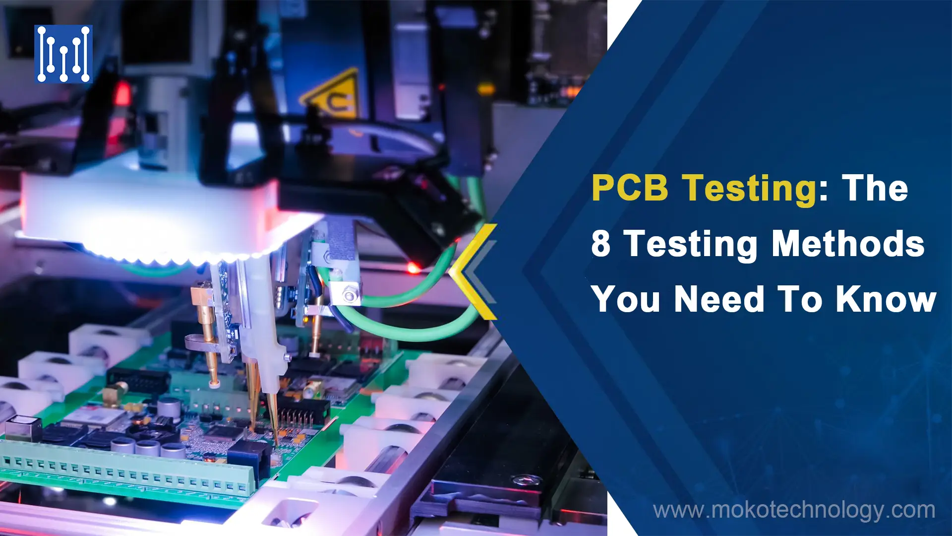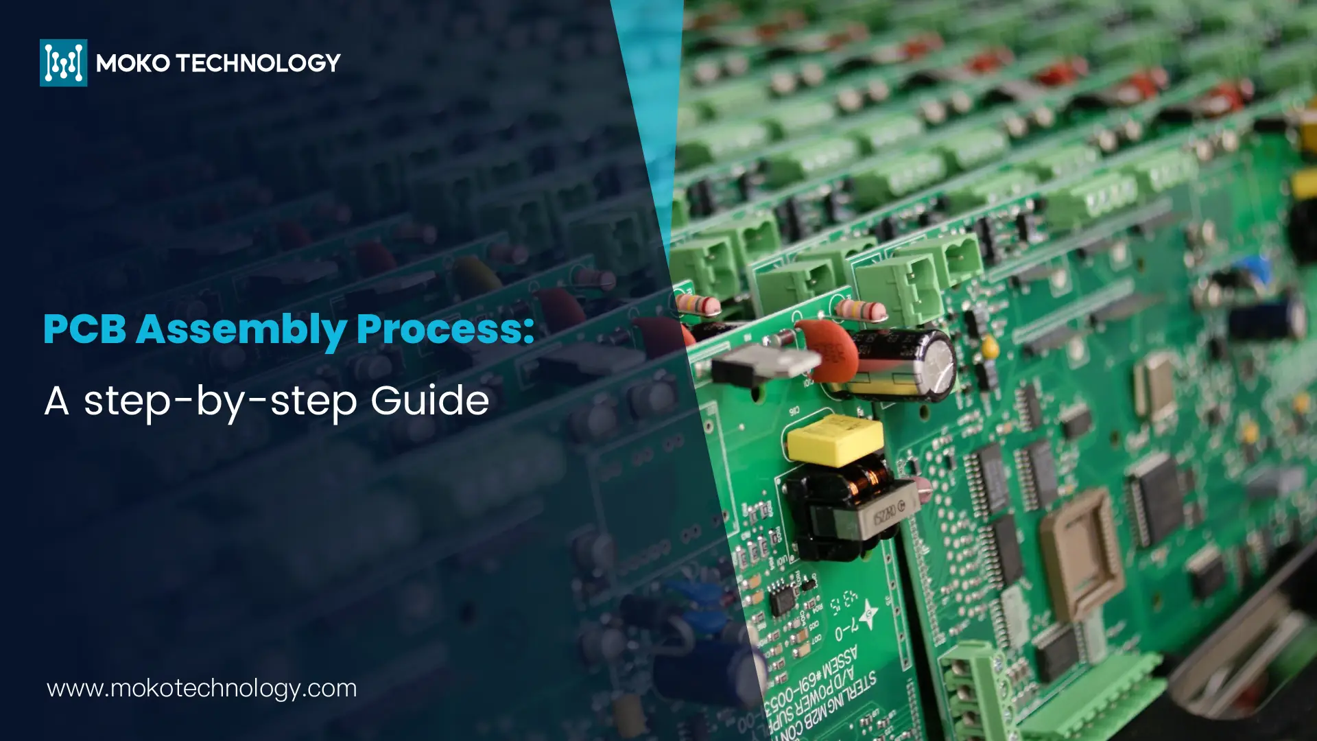
PCB assembly refers to the process of assembling all electronic components such as resistors, transistors, diodes, etc. onto a printed circuit board, and the assembly method can be manual or mechanical. In this blog, you will learn the process of printed circuit board assembly step by step.
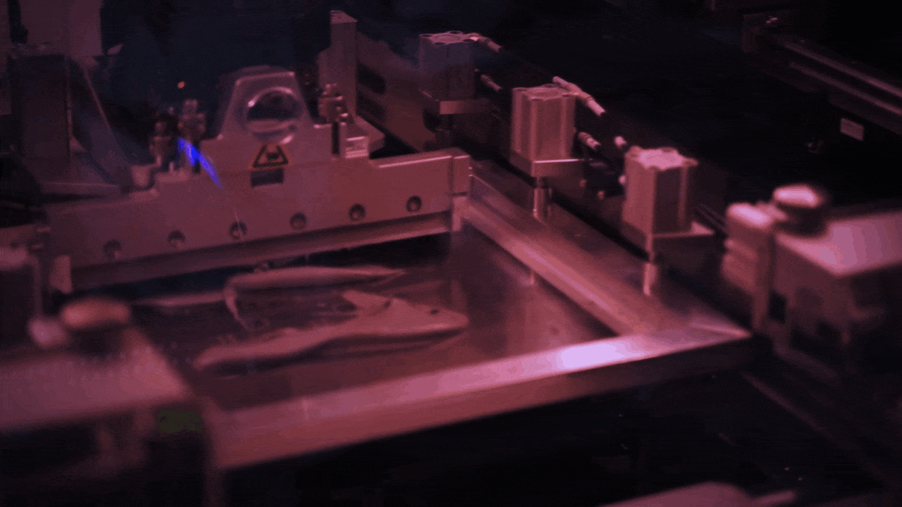
Step 1: Solder Paste Stenciling
In the first step, solder paste would be applied to the board. The solder paste is grey and consists of tiny metal balls composed of 96.5% tin, 3% silver, and 0.5% copper, be sure to use it in a controlled amount and make sure it is applied in the exact location. In a PCB assembly line, printed circuit boards and solder stencils are held by mechanical clamps and the exact amount of solder paste is applied to the desired areas. The machine will apply the slurry to the stencil until it evenly covers each open area. Finally, when we remove the stencil we can see that the solder paste remains in the correct place.
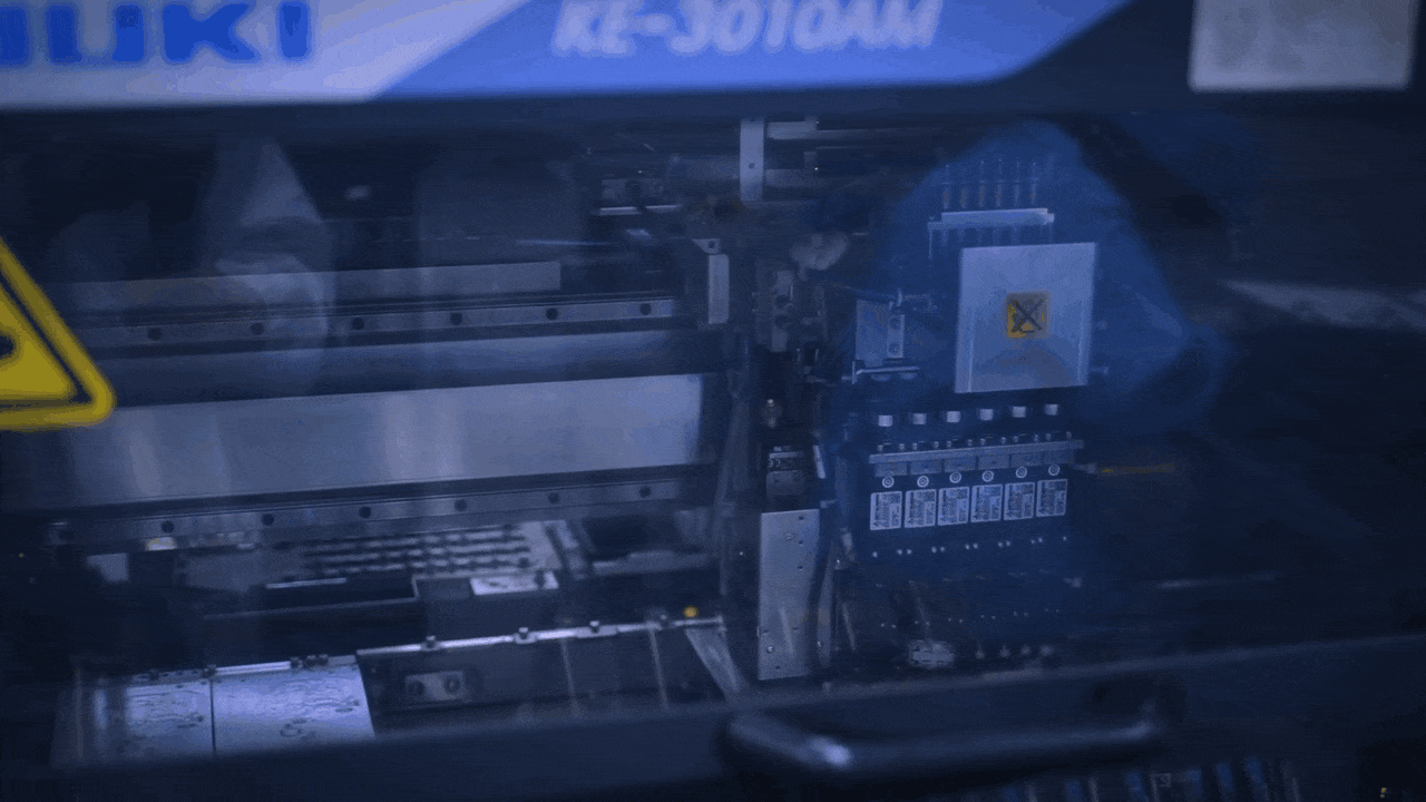
Step 2: SMT Component Pick and Place
In the second step, we need to use the pick and place machine that can place surface mount components on printed circuit boards automatically. Currently, SMD components are widely used on kinds of PCBs, which can be assembled with high efficiency. In the past, pick and place are applied manually, and the assembler need to pay much attention during the process to make sure that all components are placed in the right position. While the automatic pick and place are operated by robots that can work 24/7 without fatigue, it improved productivity and reduce errors to a large extent. The machine picks up printed circuit boards with its vacuum grip and then moves them to the pick and place station. The robot then positions the PCB on the station, and the SMD components would be placed on top of the soldering paste in intention locations.
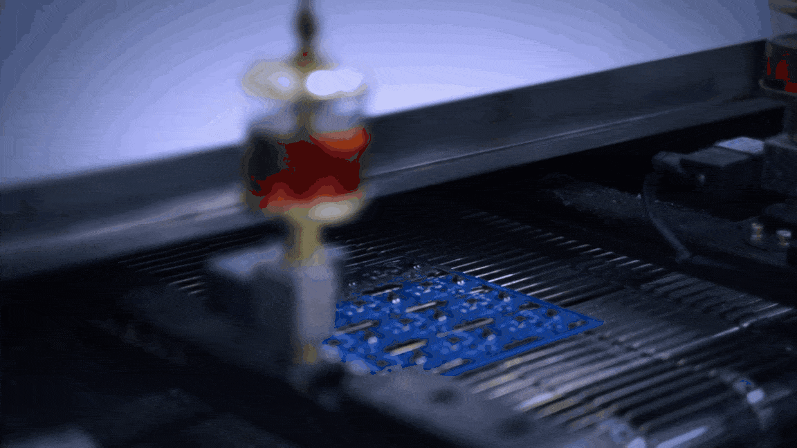
Step 3: Reflow Soldering
After the pick and place, the PCB assembly would move to the reflow soldering process. The circuit boards would be transferred to a large reflow oven through the conveyor belt. The oven would heat the boars at high temperatures, normally about 250 degrees Celsius, to melt the solder in the solder paste. When the heat process is finished, the circuit boars would be moved through the oven which consists of a series of cooler heaters, which would help to cool and solidify the melted solder. During the reflow soldering, we should pay attention to some special boards, taking two-sided PCBs for instance. Each side of two-sided PCBs needs to be stenciled and reflow soldered separately, normally, the side with fewer components would be reflow soldered first, then the other side.
Step 4: Inspection
The assembled circuit boards need to be tested for functionality the reflow process may result in poor connection or even lack of connection. The movement during the reflow soldering may also cause the shorts. Thus, inspection is a key step involved during the assembly process. There are a variety of methods to inspect errors, and the commonly used ones are manual checks, x-ray inspection, and automatic optical inspection. Periodic inspections can be performed after reflow soldering, so any potential problems can be identified until the circuit card assembly moves on to the next process. Such inspection can help manufacturers save a lot of money because the sooner they detect a problem, the sooner it can be resolved without wasting time, human resources, and materials.
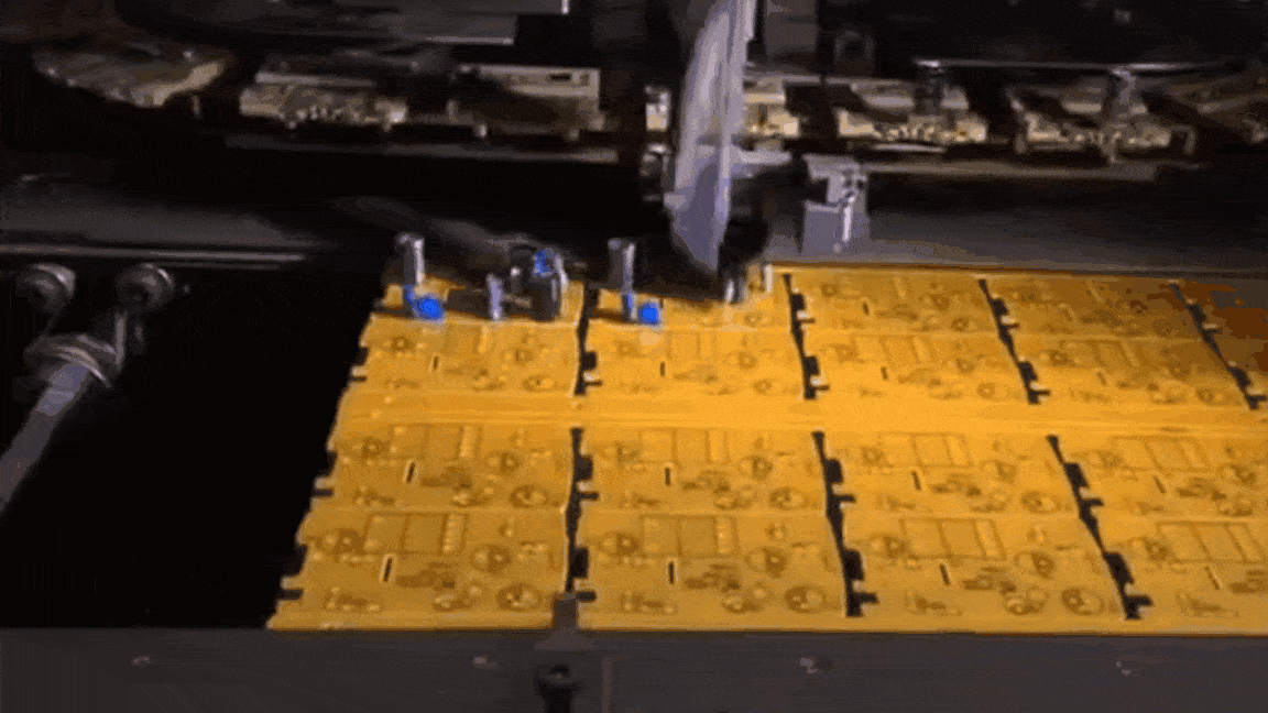
Step 5: Through-Hole Component Insertion
Apart from SMD components, some circuit boards may need to be assembled with other kinds of components like through-hole or PTH components. So how to assemble these components? These are typically inserted manually by skilled technicians. Following insertion, the boards undergo wave soldering or the selective soldering suitable for mixed technology boards. This ensures reliable electrical connections.
Step 6: Functional Test
In the last step, the final inspection will be performed to test the functionality of PCBA, we call this process a “functional test”. This test will simulate the normal operation of the PCB, and monitor the electrical characteristics of the PCB when the power supply and analog signal pass through the PCB to judge whether the PCBA is qualified.
PCB Assembly Service at MOKO
MOKO Technology is a leading PCBA provider in China, certificated with ISO9001, ISO14001, ISO13485, IPC, and UL. We are committed to providing high-quality PCB assembly service by leveraging our 18 years of experience and expertise, which make us confident to meet kinds of assembly requirements well.
Almost everything can be assembled here, we provide a full-coverage PCB Assembly service including SMT, THT, Box Build, Wire Harness, and BGA assembly. From prototype assembly boards, low-volume PCB assembly to high-volume PCB board assembly, we can always provide superior PCBA to our customers with a short turnaround time.
FAQs about PCB Assembly
Q: What is the difference between SMT and THT assembly?
SMT is done by putting the components onto the solder pads directly on the surface of the PCB and THT is done by passing the components through holes in the board. SMT is suitable for high-density components design, while THT is applied to PCBs that need firmer mechanical connections or where the power rating is high.
Q: What factors affect the cost of PCB assembly?
The following are the factors that affect the cost of printed circuit board assembly:
- Board complexity and size
- Number and type of components
- Production volume
- Turnaround time requirements
- Special processes (e.g., conformal coating)
- Testing requirements
Q: Can I assemble PCBs at home?
It is relatively easy to build simple PCBs at home, but it is best to get a professional to handle PCB assembly. Home assembly is restricted to the absence of specialized equipment for precise component placement, reflow soldering and testing. It is also difficult to achieve and constantly sustain the level of cleanliness and control that makes for reliable assembly in one’s home.
Q: What are common defects in PCB assembly, and how are they prevented?
Some of common defects are solder bridges, insufficient solder, component misalignment, tombstoning. These can be prevented through proper design for manufacturing, strict process controls, utilizing advanced assembly equipment, and performing various inspection methods,
Q: Do you provide Design for Assembly (DFA) service?
Yes, of course. MOKO Technology provides free DFA service before assembling the circuit boards to help clients reduce cost and enhance product quality. This process involves checking component positioning and orientation, standardizing components and minimizing the part counts.