Reflow soldering is widely used for manufacturing PCB assemblies. It provides consistent soldering for the large variety of required components and pad sizes. On top of that, it is very easy to control and monitor. Industries have been using reflow soldering for many years to manufacture PCB assemblies.In this guide, we will explain what reflow soldering is, how this critical process works, common reflow soldering defects, and compare it with wave soldering. Let’s read on.
What Is Reflow Soldering?
Reflow soldering is a method used to attach surface-mount components to a printed circuit board. The process begins by applying solder paste to designated pads on the PCB. Next, the components are placed onto the paste, and the assembly is heated in a reflow oven. And when the temperature goes up, solder paste will melt creating strong electrical and mechanical connections between the components and the circuit boards.
Benefits of Using Reflow Soldering
Reflow soldering allows for the simultaneous processing of multiple connections. This prevents the disconnection of wires while you are soldering their neighboring wires. Reflow Soldering also improves the quality of resulting PCB and offers many other benefits such as,
- Improved wettability of solder joints and surface mounted components.
- Improved solderability of a large variety of electronic components.
- Enhanced joint integrity for crucial electronic applications.
- Reduced board discoloration.
- Elimination of charred flux residues on heating elements and boards.
- Reduced formation of white haze from the oxidation of rosin or tin flux
- Optimized performance of low-residue and no-clean pastes.
- Enhanced flexibility of the process for accommodating a wide variety of operating conditions.
Reflow Soldering Process in PCB Manufacturing: 6 Steps Involved
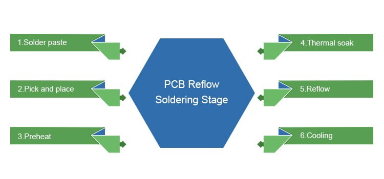
Reflow Soldering stage in PCB manufacturing involves a number of steps. We will discuss them one by one.
Solder paste
First, we apply the solder paste to the board. We apply it only to those areas which require soldering. We achieve this by using a solder paste machine and a solder mask. Once, we apply the solder paste, we can move on to the next step.
Pick and place
After applying the solder paste, we can then set components in place. Typically, we use an automated machine for picking and placing the components. This is because the manual placement is not viable due to a large number of components and required accuracy. However, it is necessary to handle components with care.
Preheat
We need to steadily bring the boards near the required temperature. If the heating rate is very high, then the components or the board will incur damage due to the thermal stress. In addition to that, if the heating rate is too high then the thermal stress won’t allow some areas of the board to reach the required temperature. On the other hand, if the heating rate is too slow then the entire board might not reach the required temperature.
Thermal soak
Once we bring the temperature of the board to the required temperature then we begin the next step. This is often known as “Thermal Soaking.” This is where we maintain the board at the required temperature. We do this for three reasons,
• To ensure that if there are any areas that haven’t reached the required temperature may do so in this step.
• For removing the volatiles and solder paste solvents.
• To activate the flux.
Reflow
The reflow step is the step of the soldering process where we achieve the highest temperature. In this step, the solder melts and creates the needed solder joints. The activated flux accomplishes metallurgical bonding by reducing the surface tension at the junction of involved metals. This allows the individual to solder powder spheres to melt and combine.
Cooling
We need to cool the boards after the reflow step in such a way that it doesn’t exert stress on the components. You can avoid the thermal shock to the components and excessive intermetallic formation by using an appropriate cooling rate. We mostly use the temperature range of 30 – 100°C for cooling the boards. This temperature range creates a fast cooling rate which can help in creating a very fine grain size. This can allow the solder to make a sound mechanical joint.
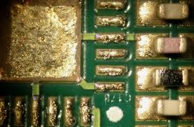
Common Reflow Soldering Defects to Watch Out For
Like any manufacturing process, reflow soldering comes with its defects. We will take a brief look at some common reflow soldering defects and how you can avoid them.
Solder Splashes
Solder splashes happen when solder paste sticks on the solder mask in muddled patterns. These are caused by the inappropriate use of the fluxing agent. It can also result from the presence of pollutants on the surface of the boards. They can be avoided by using a sufficient amount of fluxing agent and they should be prevented at all costs for they can cause a short circuit.
Solder Skips
A solder skip is a solder joint that is not properly wetted with solder. It happens when the solder cannot reach a pad and hence results in an open circuit. It is because of slip-ups in the manufacturing or design phase. You should evenly distribute the solder paste if you want to avoid solder skips.
Solder Balling
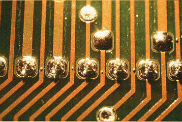
Solder balls are a common defect with reflow soldering. These are small spheres of solder paste which attach themselves to a resist, conductor, or laminate surface. These can result due to a number of reasons such as poor reflow temperature range, using rusted electronic components, improper application of solder paste, and rough PCB design.
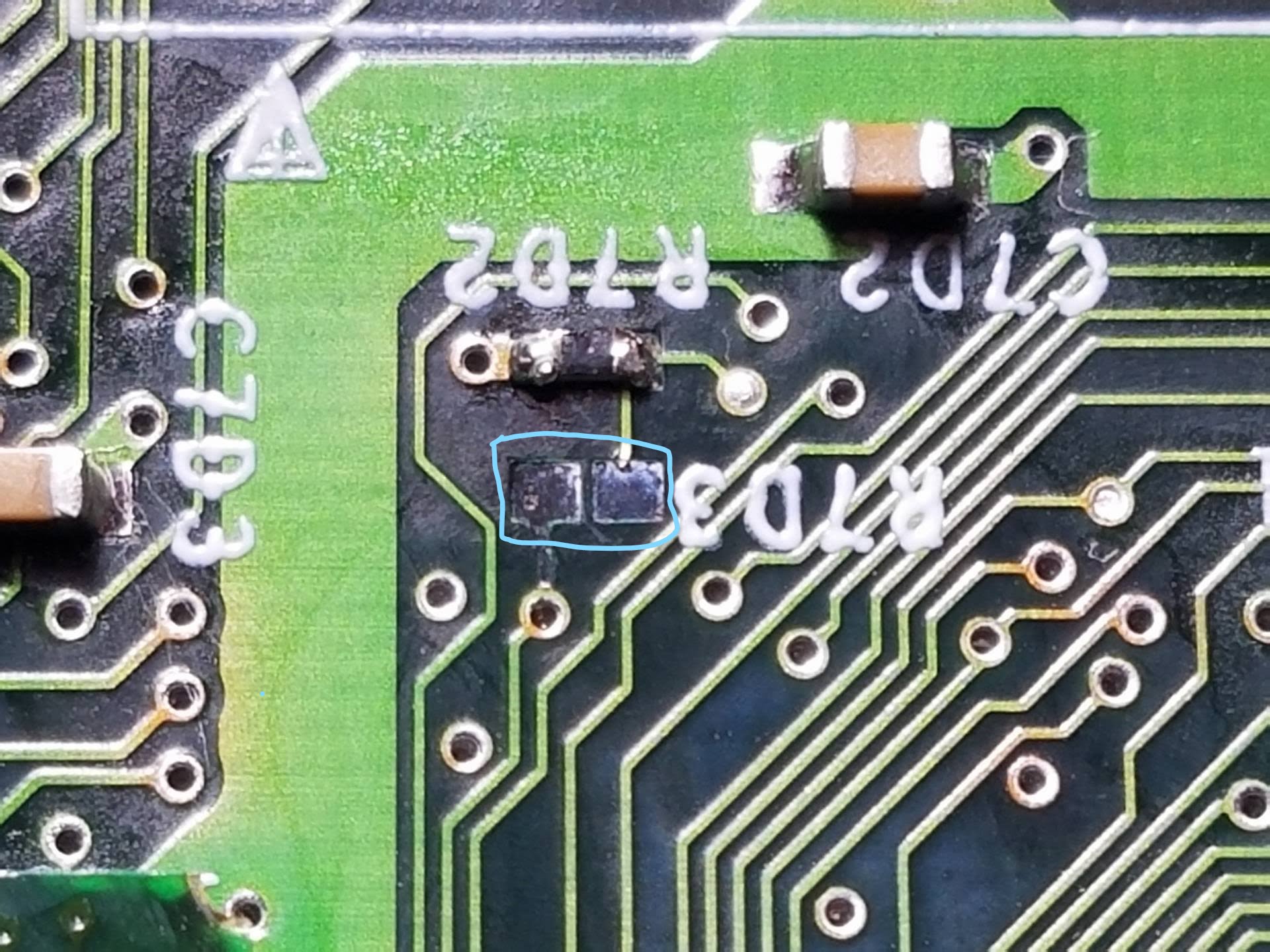
Solder Starved
A solder-starved joint is the one that doesn’t have enough amount of solder to form a viable connection. It mostly results from insufficient heating and this can lead to a breakdown of the entire circuit. Sometimes a solder-starved joint functions normal in the beginning but ultimately fails as cracks begin to develop. You can fix a solder-starved joint by simply reheating the joint and adding more solder paste.
People often confuse solder-starved joints with solder skips. However, they are not the same. Solder skips are those solder joints where solder cannot reach at all or can’t form a mechanical connection due to poor wetting. A solder-starved joint is that joint where the amount of solder is insufficient to form an electrical connection.
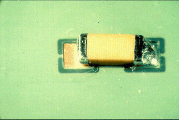
Tombstoning
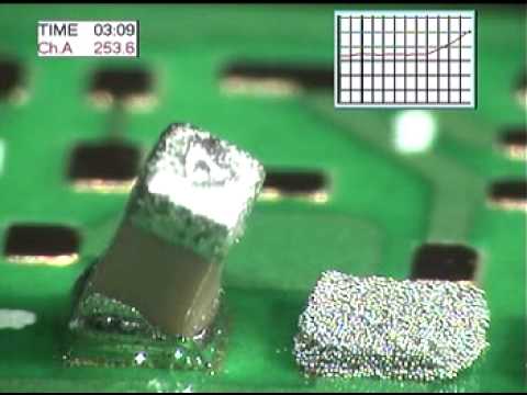
PCB Tombstone occurs when a component has one side lifted off from the pad. The solder should begin the wetting process by attaching to both pads. However, if the solder is unable to complete the wetting process on one pad then one side of the component might tilt. This will look like a typical tombstone and that is the origin of this defect’s name.
Tombstoning can result from anything that would melt the solder paste on one pad before the other. Typical causes are the uneven thickness of the traces which connect to the pad or lack of thermal relief design. If components have a large body then they may slip in solder paste and this can fix them in the shape of a tombstone.
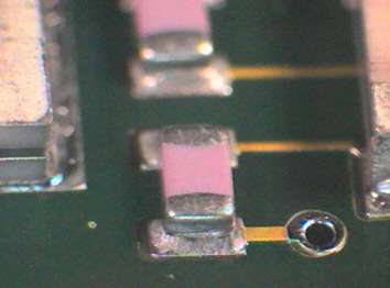
Solder Bridging
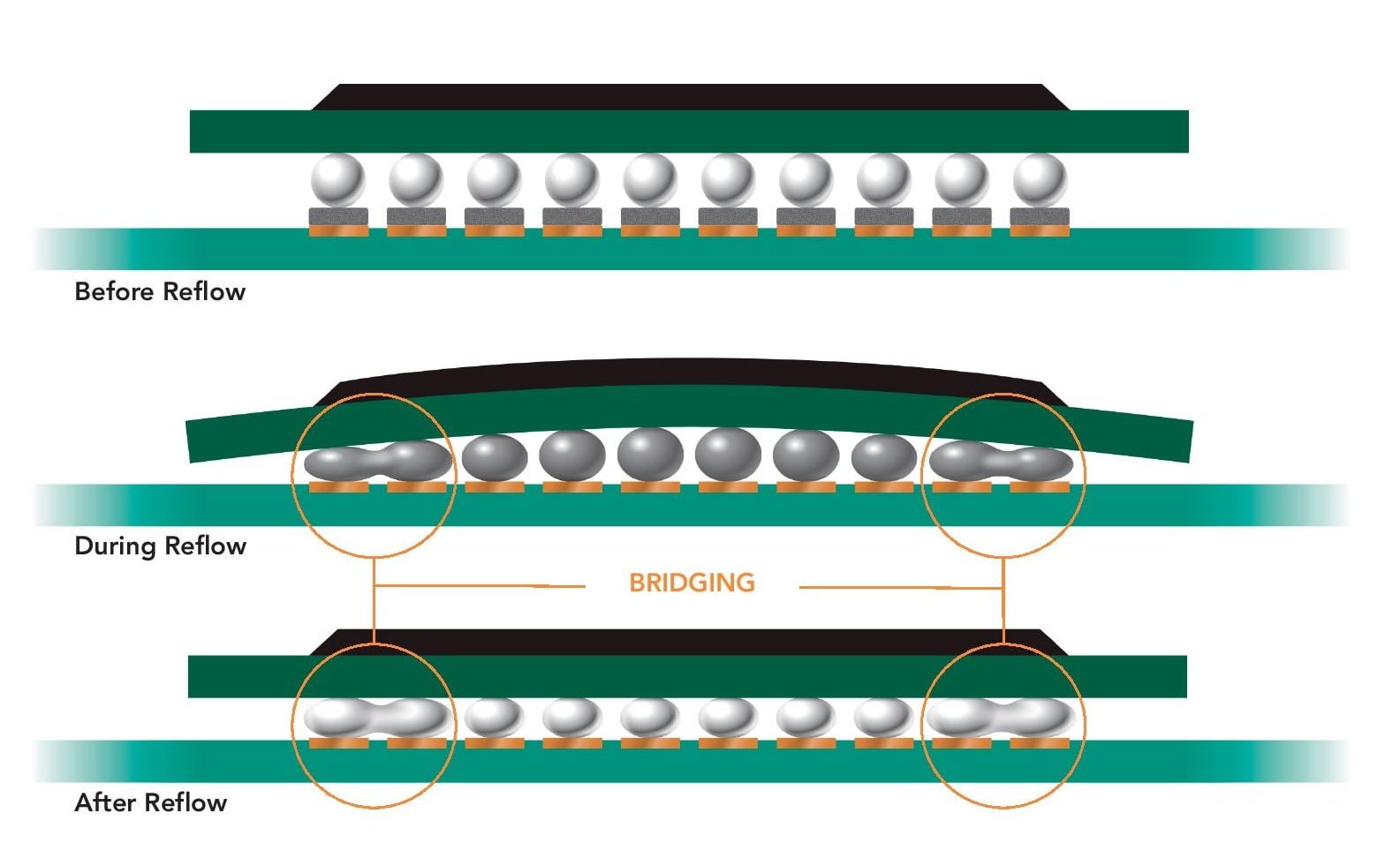
Many problems can arise from using small components and solder bridging takes the top spot in this regard. Solder bridging happens when two or more solder joints accidentally connect with each other. This happens mostly because of using big or wide soldering tips and applying too much solder paste. It is often difficult to join a solder bridge because these are sometimes microscopic in nature. If we are unable to detect a solder bridge then it can result in a short circuit and can burn or damage the components.
We can fix a solder bridge by holding the soldering iron in the middle of the solder bridge. This will melt the solder and we can draw it through for breaking the bridge. We can use a solder sucker if the solder bridge is too large.
Lifted pads
Lifted pads are those solder pads that are detached from the surface of a PCB. This mostly happens due to excessive heating or large force on a solder joint. It is difficult to work with such pads because the pads are quite delicate and can tear away from the surface. You should make every effort to attach the pad back onto the PCB before you attempt to solder it.
Reflow Soldering Vs. Wave Soldering: What’s the Difference?
There are two different processes used to assemble a PCB: reflow soldering and wave soldering, each suited for different types of components and manufacturing needs.
For the most used field, reflow soldering is predominantly used for placing surface mount components. It is an excellent method for small, delicate, and high density components.
On the other hand, wave soldering is a conventional process for through hole components in which the PCB is traversed across a wave of molten solder to weld the component’s leads to PCB pads. While reflow soldering achieves greater precision for fine pitch components, wave soldering is more effective for large-scale production of through-hole components, especially when combined with selective soldering for mixed component assemblies.
In a word, when choosing the soldering technique, the type of components on the PCB, assembly complexity and desired production volume determines the choice of these methods.
Bottom Line
Reflow soldering is a process that requires expertise and advanced equipment, as precise temperature control and careful handling are critical to ensure strong, reliable solder joints. The right setup and skilled technicians are essential to avoid defects and achieve optimal results. MOKO Technology has 8 automatic SMD assembly lines and a state-of-the-art reflow soldering setup. With our vast production capacity and highly trained technicians, you can trust us to handle the complexity of reflow soldering with precision. If you lack the resources for proper reflow soldering of your PCBs or you simply don’t want to indulge in its sophistication then feel free to reach out to us.