PCB(Printed Circuit Board) is no longer strange to us, which is a core part of electronic devices such as cellphones, computers, radios, and lights. Without the development of PCB, there would be no way that we could enjoy the convenience brought from these electronic devices. Then, a question comes to my mind: What is the development history of PCB? Well, let’s discuss it in this article.
Milestones in the Development Process of PCB History
We can learn the PCB development process by dividing it into several vital stages which are listed below:
Budding Stage(1900s-1920s):
In 1903, a famous German inventor named Albert Hanson applied for a British patent, and he pioneered the concept of using “wires” used in the telephone exchange systems, the metal foil is used to cut line conductors, and then paraffin paper is glued on the top and bottom of the line conductors, and via holes are set at the line intersections to realize the electrical interconnection between different layers. This is different from our modern PCB manufacturing method, because phenol resin has not yet been invented at that time, and the chemical etching technology is not yet mature. The method invented by Albert Hansen can be said to be the prototype of modern PCB manufacturing, which is a base for the following development.
Developing Stage(1920s-1940s):
In 1925, Charles Ducas came from the United States who had an innovative thought to print circuit patterns on a substrate of insulating, and then plating was applied to make conductors for wiring. The term “PCB” emerged at this time. This method makes it easy to manufacture electrical appliances.
In 1936, the Austrian Dr. Paul Eisler, known as “the father of printed circuit”, published foil film technology in the United Kingdom who developed the first printed circuit board for use in a radio set. And the method that Paul Eisler used is very similar to the way that we use for today’s printed circuit boards. This method is called subtraction, it can remove the unnecessary metal parts.
Around 1943, Paul Eisler’s technical invention was used on a large scale by the United States to make proximity fuzes for use in World War II. At the same time, the technology is widely used in military radios.
Turning Point(1948):
The Year 1948 is a turning point in the process of PCB history development, as the United States officially recognized the printed circuit board invention for commercial use. Although there are little electronic equipment using PCB history at that time, this decision promoted the development and application of PCB in a large part.
Flourishing Stage(1950s-1990s):
From the 1950s to the 1990s, the PCB industry was formed and rapidly growing, that is, the early stage of PCB industrialization, at which time PCB has become an industry.
In the 1950s, transistors are used in the electronics market, which helped to reduce the size of electronics effectively and make it much easier to incorporate PCBs, in addition, the electronic reliability was improved significantly.
In 1953, a double-sided board with electroplated vias was developed by Motorola. Around 1955, Toshiba of Japan introduced a technology to generate copper oxide on the surface of copper foil, and copper-clad laminate (CCL) appeared. Thanks to these two technologies, the multi-layer printed circuit boards were invented successfully and have been used on a large scale.
In the 1960s, printed circuit boards were widely used at this time, PCB technology was more and more advanced, and thanks to the wide use of multiple layers printed circuit boards, the ratio of wiring to substrate area was increased efficiently.
In the 1970s, there is a rapid development of multi-layer PCBs, aspiring to higher precision and density, small holes with exquisite lines, high reliability, lower cost, and automatic production. At that period, the PCB design work was still done manually. The PCB Layout engineers used colored pencils and rulers to draw circuits on transparent polyester film. In order to improve drawing efficiency, they made several packaging templates and circuit templates for some common devices.
In the 1980s, surface mounting technology(SMT) began to gradually replace through-hole mounting technology and become the mainstream in that time. It has also entered the digital age.
Mature Stage(1990s-Now):
With the development of electronic devices such as personal computers, CDs, cameras, game consoles, etc., great changes have taken place accordingly. The size of PCBs must be decreased to fit these small electronic devices.
Computerization design achieved automation in many steps in PCB design and made it easier for designs with small and lightweight components. As regards the component suppliers, they need to improve their devices as well by reducing their electrical consumption, but at the same time, they need to consider the cost reduction question.
In the 2000s, PCBs became more complex with more functions while the size became smaller. Especially the multi-layer and flex circuit PCB designs made these electronic devices much more workable and functional, with small size and lower cost PCBs.
Early 21st century, the emergence of smartphones drove the development of HDI PCB technology. While retaining the laser-drilled micro vias, stacked vias began to replace the staggering vias, and combined with “any layer” construction technology, the final line width/line spacing of the HDI board reached 40μm.
This arbitrary layer method is still based on a subtractive process, and it is certain that for mobile electronic products, most high-end HDI still use this technology. However, in 2017, HDI began to enter a new stage of development, beginning to shift from a subtractive process to a process based on pattern plating.
Main Trends Would Impact the PCB Industry
Nowadays, various types of printed circuit boards including rigid PCB, rigid-flex PCB, multi-layers PCB, and HDI PCB are widely used in the market, which are experienced many times evolution. What we can confirm is that such evolution would continue in the future along with the constantly improved requirements from people.
So, here comes another question, have you ever considered what trends will PCB develop towards? Along with the emerging electronic product applications in the consumer market, such as wearable electronic devices, electronic hearing aids, blood glucose meters, intelligent devices for electric vehicles, aerospace, and other fields, people have higher requirements of PCB design, material, and manufacturing. Below are 5 main trends that would affect the PCB industry in the future:
Internet of Things
Internet of things, IoT for short, is an industry with a brilliant and limitless future. This technology brings every object to the Internet, and each object can communicate with each other by sharing data with. It makes people’s life more smart and convenient. Normally, IoT devices should be equipped with sensors and wireless connectivity. Thus, it is necessary to evolve PCB to meet these requirements.
For example, those IoT devices with small sizes such as BLE bracelets or other portable devices need tinier components with the same functionality. Then for PCB, they should be getting smaller while it should equip even more complex components at the same time. This can be a challenge but an opportunity for PCB manufacturers if they want to enter the market of IoT and profit from it.
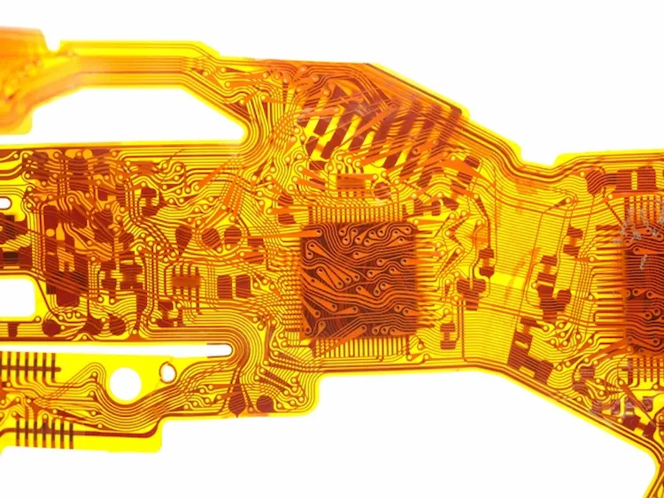
Flex PCB
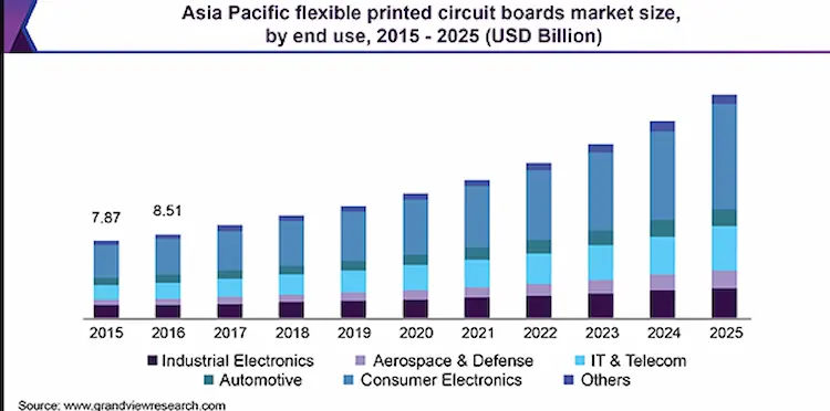
In recent years, flex PCBs are rapidly gaining market share in PCB development, let’s check the below picture from https://www.www.grandviewresearch.com, which shows the market size of flexible printed circuit boards in the Asia Pacific from the year 2015 to 2025. What we can get from it is that the total market scale is increasing continually, the industries that the flex PCBs used range from electronics and Telecom to aerospace and automotive. The demand for flex PCBs would be incredibly increasing as time goes by.
So why are flex PCBs such popular? Here are some reasons: On the one hand, the flex PCBs can save space as they are smaller than other types of PCBs. On the other hand, they can withstand tough environments with increased capability and better reliability.
High-Density Interconnect(HDI) PCB
The advantages of High-Density Interconnect PCBs are including their reliable and high-speed signal, small size, and lightweight as well. In addition, the trace widths in HDI PCBs are much smaller and the wiring density is better, so engineers can pack more function and power into even a small space. The need for layering is reduced for HDI PCBs, so the cost of production can be reduced accordingly. With so many excellent characteristics, HDI PCBs are becoming vital components in many devices and applications.
At present, people prefer to use automatic devices which are available everywhere including but not limited to aerospace applications, military communications medical diagnostic tools, and wearable technology. Meanwhile, smaller parts with faster signals were more and more needed, that’s the reason why we need those High-Density Interconnect PCBs.
High Power PCB
High-power PCB is a type of PCB that can manage voltage above 48V, they are becoming thinner and lighter with higher efficiency, better heat absorption capability, and durability. The newest high-power PCBs can withstand more heat with improved heat dissipation. With an improved battery package, this kind of PCB is able to operate much longer.
The emergence of this trend is because of the increasing need for electric vehicles which require voltages often in the hundreds. In addition, more and more people respect the sustainable concept, thus, the need for solar panels is growing increased accordingly, which require the voltage at 24V or 28V. In a word, high-power PCBs have a wider range of applications in nowadays and the future.
Commercial-Off-The-Shelf Solutions
Another trend in the PCB history industry is the commercial off-the-shelf solutions, also known as COTS, including PCB modules, components, and boards. The highlight of COTS components is that they are designed to be easily installed into existing systems, which would be very convenient. The use of it is considered to be able to make the components more standard and reliable. So you must be wondering what kind of application that people use COTS, in fact, aerospace is one main area in which COTS is used to reduce the costs of major initiatives, keep the guarantee of quality and safety while completing projects more quickly.
Conclusion
Looking back on the development process, the PCB history industry is constantly updating and evolving. PCBs play an important role in this modern-day as technology is improving constantly, no matter what these trends would bring to us, there is one thing that would never change – PCBs will always be in need.
However, along with the evolution and development in the PCB industry, a dramatic impact on both design and manufacturing would come along. Hence, if the printed circuit board manufacturers want to stay competitive, they need to be innovative to keep up with the trend including making changes to PCB assembly, design, and manufacturing to meet the increased needs of people.
MOKO, as a leading PCB designer and manufacturer in China, has over 16 years of experience in the PCB industry and owns a professional R&D team. We always follow up the trend in the PCB industry. Got any questions about PCB? Contact us, let’s dive into the PCB world together!