Printed circuit boards (PCBs) form the essential infrastructure of contemporary electronics, providing a platform for the integration and interconnection of electronic elements. Although functionality and electrical performance are paramount, the aesthetic appeal and legibility of information on a PCB are equally significant. This is where the utilization of silkscreen becomes crucial. In this article, we will dive into the world of PCB silkscreen, introducing its significance, printing methods, design considerations, and so on.
What Is Silkscreen on PCB
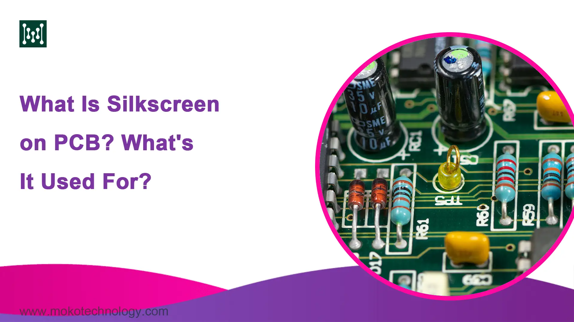
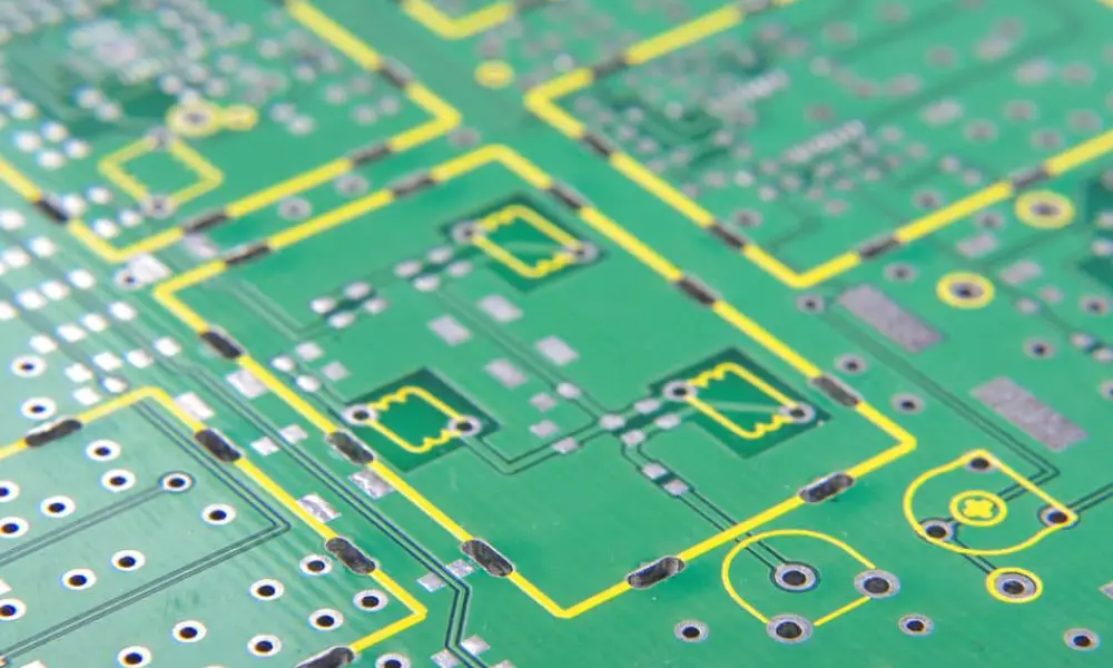
The silkscreen on a PCB is a layer of ink traces that serve multiple purposes. It includes labels for various components such as connector names, resistor, and capacitor values, as well as other information like the PCB’s title, part polarities, and test point locations. This layer is applied to the component part of the printed circuit board. Apart from its practical benefits, the silkscreen also has a visual function. It can incorporate branding elements, company logos, and decorative features to enhance the overall appearance of the PCB, making it more appealing and professional. The ink used for the silkscreen layer is typically a non-conductive epoxy ink available in various colors such as black, white, red, blue, and yellow. In addition, the silkscreen is a vital aspect of PCB design and plays a crucial role in the functionality of electronic circuits. Whether it’s a complex circuit designed by an engineer or a simple project assembled by a hobbyist, the silkscreen aids in the efficient assembly and troubleshooting of the circuit. It is positioned as the topmost layer of the PCB and serves as a reference for component placement, providing valuable information during the PCB assembly process. The ink used for silk screen printing on PCBs is specifically formulated with a heat and chemical-resistant resin to withstand the soldering and assembly processes.
Methods of Applying PCB Silkscreen
The choice of the silkscreen method depends on various factors, including time, price, material, required accuracy, and board spacing. In this section, we will present three commonly employed PCB screen printing methods.
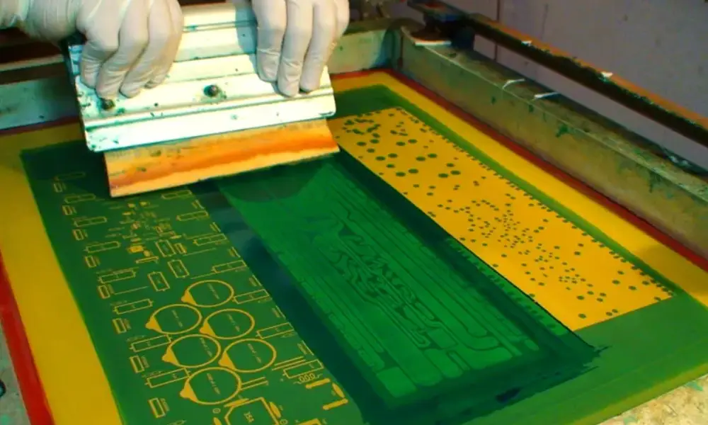
Manual Screen Printing
The manual screen printing method is considered the oldest and most cost-effective approach for PCB silkscreen printing. Epoxy ink is utilized in this process, where the ink is manually applied to the laminate and subsequently dried to achieve the desired impression on the PCB. One significant advantage of the manual screen printing method is its relatively manageable setup requirements, making it a preferred choice for many applications. However, it should be noted that this method is better suited for larger board sizes due to the dominant text size associated with it, requiring sufficient space for the impression to dry effectively. If the objective is to minimize expenses and board spacing is not a constraint, it is advisable to opt for the manual screen printing method.
Liquid Photo Imaging (LPI)
Liquid photo imaging involves coating the laminate with epoxy, which possesses photo imaging properties. Subsequently, the silkscreen sketch is conveyed to plates by exposing them to ultraviolet light. Liquid photo imaging yields higher precision compared to the manual silkscreen method and requires less space for implementation. However, this method consumes more ink and setup time than alternative screen printing methods. When prioritizing PCB space conservation and achieving finer results, it is advisable to consider the liquid photo imaging method.
Direct Legend Printing (DLP)
The direct legend printing method employs inkjet printers to transfer ink onto PCBs, similar to paper printers. This method allows for direct printing of CAD application information onto the board. It offers high accuracy and time efficiency, with a text height capacity equal to or greater than 0.02 inches. It is important to avoid using heights below 0.02 inches as they may be difficult to read. However, there are limitations to consider with the direct legend printing method. It is not suitable for PCBs made with silver materials, and there may be restrictions on the use of acrylic ink in certain cases.
The table below makes comparison among these three techniques in terms of different aspects:
| Silkscreen Technique | Manual Screen Printing | Liquid Photo Imaging (LPI) | Direct Legend Printing (DLP) |
| Process | Manual process using a stencil and squeegee to apply ink | Photographic process using a photosensitive emulsion and UV exposure | Inkjet printing directly onto the PCB |
| Precision | Moderate precision | High precision | High precision |
| Resolution | Limited resolution | High resolution | High resolution |
| Complexity | Requires skilled operator | Requires specialized equipment and chemical processes | Requires compatible inkjet printer and software |
| Time Efficiency | Moderate speed | Moderate to high speed | High speed |
| Setup Cost | Low | Moderate to high | Moderate |
| Text Height Capability | Moderate | Very fine | Very fine |
| Compatibility | Works with various PCB materials and ink types | Works with various PCB materials and ink types | May have limitations with certain PCB materials and ink types |
| Versatility | Suitable for low to medium volume production | Suitable for medium to high volume production | Suitable for low to medium volume production |
| Aesthetics | Can produce slightly rougher edges | Can produce sharp and precise edges | Can produce sharp and precise edges |
| Component Interference | Potential for interference if not carefully aligned | Minimal interference due to high precision | Minimal interference due to high precision |
The Benefits of Silkscreen Markings on PCBs
- Component Identification
Silkscreen markings provide clear labels for components such as connectors, resistors, capacitors, and integrated circuits. These labels help users easily identify and locate specific components during assembly, testing, and troubleshooting processes.
- Reference for Component Placement
Silkscreen markings serve as a visual guide for accurate component placement during PCB assembly. They indicate the designated positions for components, ensuring proper alignment and reducing the risk of errors or misplacements.
- Improved Clarity and Readability
Silkscreen markings enhance the legibility of important information on the PCB. Clear and properly aligned text, symbols, and graphics make it easier for technicians, engineers, and users to interpret the board’s specifications, part numbers, reference designators, and other essential details.
- Error Prevention and Quality Control
Silkscreen markings aid in error prevention and quality control during the manufacturing and assembly processes. By providing visual indicators, they assist in identifying any incorrect or missing components, reducing the likelihood of production errors, and improving overall product reliability.
- Branding and Professional Appearance
Silkscreen markings can incorporate branding elements, company logos, and decorative designs onto the PCB. This imparts a sophisticated impression of the end product and amplifies brand awareness.
- Enhanced Troubleshooting and Maintenance
Silkscreen markings facilitate troubleshooting and maintenance tasks by providing valuable information on component values, pin configurations, test points, and polarity markings. This enables technicians to quickly identify and address any issues, minimizing downtime and improving the overall efficiency of repairs.
Design Considerations for Silkscreen on PCBs
When designing the silkscreen for a PCB, several crucial factors need to be taken into account. These include:
Size and placement: The size of the silkscreen should strike a balance between readability and conserving space on the PCB. It should possess adequate size for effortless readability without excessive dominance. Additionally, the positioning should guarantee clear visibility and prevent any disruption or obstruction to other components on the PCB.
Font and style: Select a clear and legible font for the silkscreen text that is consistent throughout the PCB. Avoid using overly elaborate or complex fonts that may hinder readability.
Color: Carefully choose the color of the silkscreen. Dark colors like black or dark blue are generally easier to read, but the suitability may vary depending on the specific application or requirements.
Information: Include only essential information related to the circuit and its components on the silkscreen. Avoid redundant details or duplicating information already present elsewhere on the PCB to maintain clarity and avoid confusion.
Key Takeaways
Silkscreen on PCBs is a vital component of modern electronics, providing both practical and visual benefits. By carefully considering design aspects and employing appropriate silkscreen techniques, manufacturers can enhance the functionality, readability, and aesthetic appeal of PCBs. MOKO Technology is a leading PCB manufacturer in China that understands the intricacies of silkscreen and can help you save time and costs on your PCB projects. With our experience and manufacturing capabilities, we ensure precise silkscreen application and high-quality PCB production. Contact us today to see how our comprehensive PCB manufacturing services can benefit you.