PCB manufacturers are increasingly concentrating more on designing smaller printed circuit boards. Moko Technology isn’t left out; we integrate fewer through-hole components while incorporating more surface mount technology (SMT). For large plated through-holes, we are assigning less space on the board. Instead of plated through-holes, we are increasingly using SMT components. All our PCBs are designed to use vias.
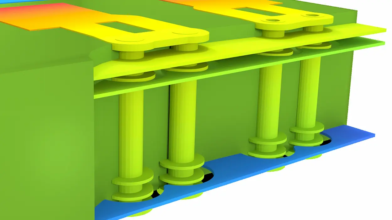
A via refers to a plated-through hole found in PCBs used to track a trace from the surface layer of the board to the interior and other layers. PCB vias can be plated to form electrical connections, and they can be drilled mechanically.
Although vias are essential in multi-layered PCB boards, it is challenging to design and produce them. They build paths for the thermal current and electrical flow between the different layers of the board. Essentially, vias are channels that differ in type and magnitude.
Types of PCB via
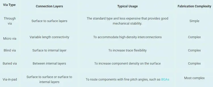
There are 5 PCB via types. They are;
1. Blind via – A blind via is a laser that transits from only one layer to the next.
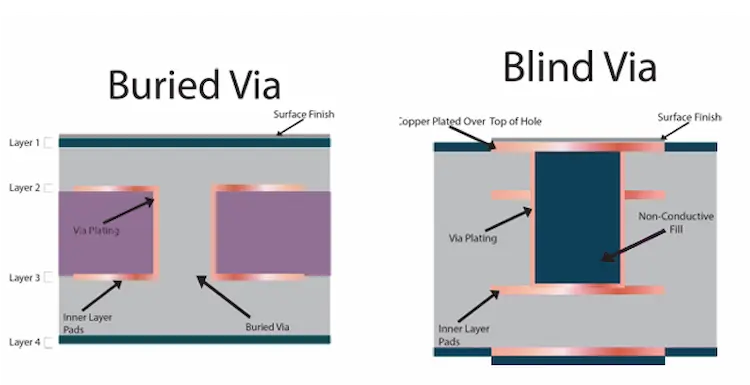
2. Buried via – This type of a via is between internal layers and is required when sequential or multi-lamination projects exist.
3. Through via – A through via links the two outer layers by drilling from top to bottom.
4. Micro-via – Micro-via is drilled using a laser rather than mechanically drilling, allowing less than 0.006 inches.
5. Via-in-pad – This via is positioned inside the surface mount component’s pad.
Blind Via vs. Buried Via
The buried and blind are used to link different layers of a PCB. The buried via offers inner layer interconnection as the board is entirely hidden from the PCB’s outer surroundings. At the same time, blind vias provide an external layer interconnection with one or many internal PCB layers. These two vias are beneficial in HDI PCB because their ideal density is deprived by increasing the board’s size or increasing the PCB board’s layers.
PCB Micro-via
Micro-vias can be drilled using lasers as their diameter is smaller than through-hole vias diameter. As it is hard to plate copper inside micro-vias, they only have a depth of fewer than two layers. Hence, when the diameter of a Via is small, the throwing capacity of the coating bath becomes higher, thereby creating an electroless copper coating.
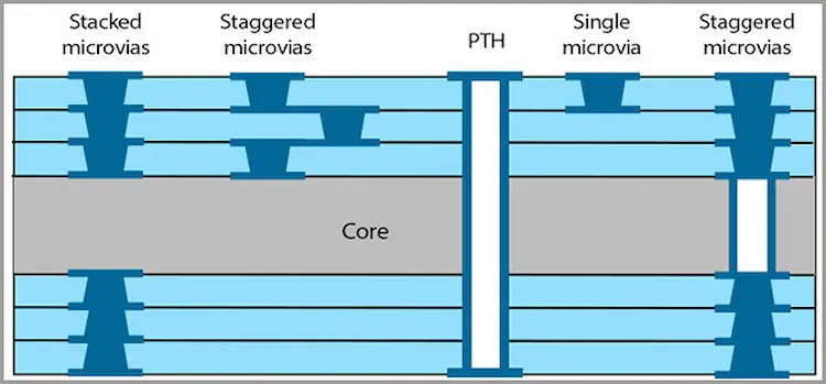
According to their locus in the board layers, micro-vias are categorized into either stacked skip or staggered.
• Stacked vias – They can be created by stacking them above each other in different layers.
• Staggered vias – These vias can be scattered in several layers, although they are costly.
• Skip vias can be passed through a layer, making sure that the layer has no electrical contact. Hence, a skipped layer cannot form an electrical link with a via.
PCB Via-in-pad
The Via-in-pad method was invented because of the high signal speed and the thickness and density of PCB components. Standard via structures and VIPPO can make the routing capability and integrity features of a signal.
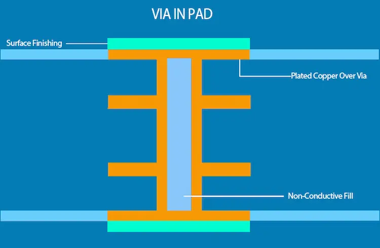
The signal trace of standard vias is traced from the pad to the via by manufacturers to avoid solder coat leakage into the vias. A via in via-in-pad is placed in the external mount component’s pad.
This is done by first filling the via using non-conductive epoxy depending on the requirements of the PCB manufacturer. Then, the via is, and the coat is caped to retrieve land space. Due to this, the signal path expands, thus eliminating the effect of opportunistic inductance and capacitance.
More importantly, the via-in-pad reduces the size of the PCB board and hosts the size of a small ground. This method is most suited for components of a BGA footprint. It is essential to implement the back-drilling process using a via-in-pad when aiming to achieve great results. The signal echoes found in the remaining parts of a via are removed by back-drilling.
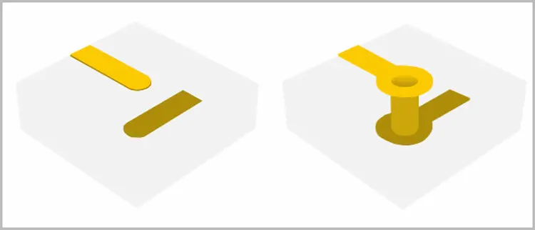
Components of a PCB via
a) Barrel- It is a conductive pipe used for filling the infiltrated hole.
b) Pad- It connects all ends of the barrel to its traces.
c) Antipad- This is a clearance hole used to separate the non-connective layer and the barrel.
Common uses of vias in PCB design
• Signal routing – A large number of PCB boards use the through via for signal routing. However, thicker boards use buried or blind vias, whereas light boards only use micro-vias.
• Power routing – Vias in most PCB boards are restricted using broad through-hole vias for power and ground nets routing, although blind-vias can be used as well.
• Escape routing – Components of the larger surface mount (SMT) mostly use the through-hole vias for escape routing. Micro-vias or blind vias are the most commonly used for escape routing, but a via-in-pad can be used on solid packages like high pin-count BGAs.
• Stitching – Through-hole or blind vias can be used to offer numerous connections to a plane. For instance, a strip of metal with vias stitched surrounds the circuitry sensitive area to link it with a ground plane for EMI protection.
• Thermal conduction – Vias can be used for thermal conduction from a component out through its connected interior plane layer. Usually, thermal vias require a dense blind via or a through-hole via where these vias must be in the pads of these devices.
Importance of vias when designing a PCB
When you have a simple circuit board, vias are not necessary. However, vias are only required when dealing with a multi-layered board. When designing PCB boards, vias are essential as they;
• Help you create an outstanding density of the components in multi-layered boards.
• Increase the trace density in multi-layered boards as they can be run above and below one another in various directions. Vias permit different traces to connect, thereby acting as vertical connection factors.
• When a via is not integrated with the routing process of a multi-layered PCB, the components end up being placed compactly.
• Facilitate power and signal transmission between the layers. PCB components should be routed on a single plane whenever you do not want to use a via. More importantly, the surface-mounted components in a multi-layered PCB make it difficult to route the parts on a single plane.
PCB design tips for vias
When using vias in a PCB, it is essential to consider the tips below;
• When designing PCBs, it is necessary to employ maximum via structures.
• When stacking between staggered and stacked vias, consider staggering vias as stacked vias must be filled.
• Reduce the aspect ratio as much as possible to attain an outstanding efficiency of signals and electrical performance. Moreover, minimize the EMI, noise, and crosstalk.
It is advisable to use smaller vias as they;
• Allow you to build a quality HDI board by reducing the inductance and capacitance of a stray.
• Fill via-in-pads every time, except when they are inside thermal pads.
• Always remember that the pad matrix where the BGA is fixed may contain blind or through-hole vias. When knowing this, make sure you planar and fill the vias to shun solder joints compromising.
• When designing PCBs, it is essential to know that vias assist in securing the solder joints of the bar and thermal from blocking the set, which hinders the formation of excellent solder joints inside the QFN joints.
• When dealing with thermal pads, use an assembly shop rather than a through-hole. It is only be attained by introducing openings with a windowpane design inside the solder coat stencil above the pad. This eliminates the effect of outgassing and solder merging during the designing process.
• Use the BGA package’s location to always lookout for a via clearance and the least trace in the routed components.
• Always fill the assembly of your via-in-pad.
• Use a pre-determined short trace to separate a via from its pad when assembling a dog bone.
• A PCB documentation requires a drill template that has X-Y points for every hole and feature code.
Via Treatment
PCB manufacturers add extra treatment on vias to help increase the PCB’s thermal performance. These additional treatments also help eliminate several assembling issues such as filling, covering, plugging, and conductive filling. Suitable treatments on vias are essential as they assist in eliminating costly troubleshooting works.
A) Covering -. It is a typical process that fabricators use to dry film solder masks. The dry film has a thickness of 4 mm, sufficient to cover even large holes effectively.
B) Filling – Fabricators use the non-conductive epoxy paste to fill a regular or an encroached via. These filled vias have a few millimeters that stop the solder mask from reaching the pad. It is an excellent technique for use in PCBs of medium density as the solder mask minimizes the chances of solder bridging between the pad and the via.
C) Plugging – This treatment involves plugging the via ends with a non-conductive epoxy paste to prevent wicking or solder flow-through during the soldering process. For the epoxy to drill the hole effectively, the via diameter must be less than 20 mm. Fabricators use a solder mask to cover the plugged via.
D) Conductive filling – PCB fabricators use pure copper or epoxy resin with copper to fill micro-vias with a conductive paste, enhancing the PCB’s conductivity. The conductive filling technique can be used for all types of vias.
Conductive vs. non-conductive via fill
PCB manufacturers use a unique manufacturing method called Via Fill to close via holes using epoxy entirely. Some key benefits of via filling are;
• Increases the yields of assembling
• It makes the surface mounts to be more reliable
• Improves consistency by minimizing chances of stuck air or liquids.
Non-conductive via fill conducts power and heat using copper-plated vias. A special low shrinkage epoxy is used to fill the via. On the other hand, conductive via fill provides additional electrical and thermal conductivity using silver of copper particles dispersed all over the epoxy.
The thermal conductivity of a non-conductive fill is 0.25 W/mK, while that of a conductive fill ranges anywhere from 3.5-15 W/mK. In contrast, the thermal conductivity of electroplated copper is more than 250W/mK.
Although a conductive via fill often provides the required conductivity in some applications, adding extra vias using the non-conductive paste is still possible. Outstanding thermal and electrical conductivity offers a less cost impact.
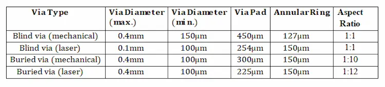
Difference between via type and via diameter
The difference in via diameter in different via types is discussed in the table below. It also clearly discusses the via pad, minimum via diameter, and annular ring of an exact PCB design layout using a via that is based on its application. Moreover, the table shows details of the different dimensions essential for implementing in the PCB. The aspect ratio of each via type is also mentioned.
Factors to consider when choosing the right via
It is essential to choose an appropriate via for any PCB project by understanding the manufacturability design. Always consider the factors below when you think of undertaking any PCB project.
1) Via type – Determine the best kind of a via for your project. When only one lamination is available without a via fill or technology, possibly there are some large holes.
2) Via size – 10 mm is the standard PCB via size or 7 mm after PCB via plating, where the board’s thickness determines the via size. Both mechanically and laser-drilled micro-vias have 4mm holes.
3) Via tolerance – It is essential to state the tolerance of the via’s hole size, although most PCB providers provide all in-house guidelines.
4) Support the most suitable technology – When you require either a buried or blind vias, always ask the PCB suppliers to create a stack-up that supports that kind of technology.
5) IPC guidelines – It is essential to follow the IPC guidelines for the allied technology strictly, like the distance in between the vias as directed by the PCB manufacturer. As the IPC assembling guidelines for military, Class 2, Class 3, and Class 3DS differ slightly, it is essential to consider them.
6) Annular ring – As the via pad’s size is quite important, it is crucial to ensure that the via has a large enough annular ring after drilling. Since mechanical drills wander a bit when drilling, the breakout drill can compromise via no sufficient annular ring.