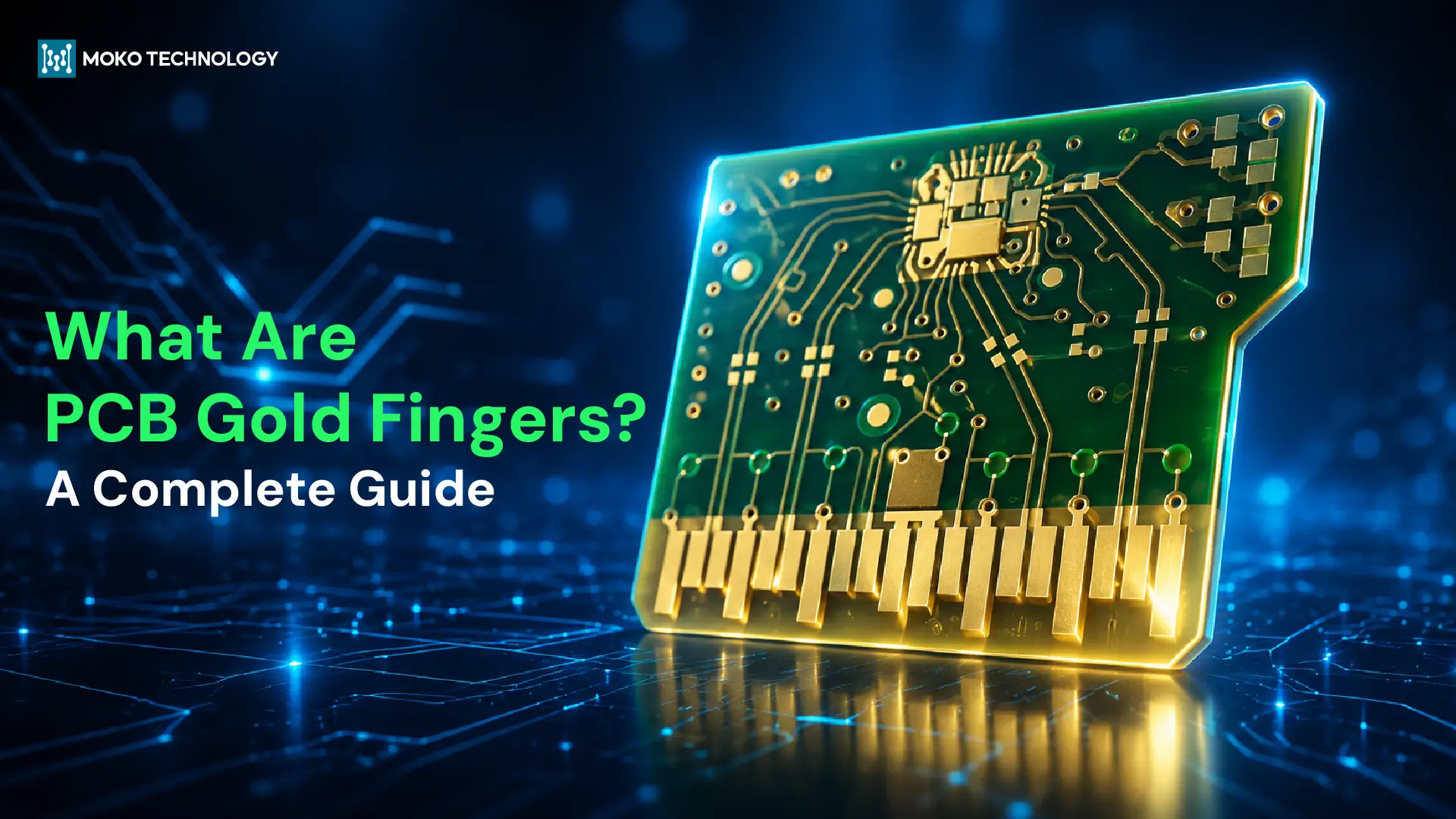
Many electronic systems use PCB gold fingers to create durable electrical connections, from graphics cards and memory modules in personal computers, to automotive electronics and industrial control devices. Located along the edge of a circuit board, these gold-plated contacts allow power and signals to transfer between a circuit board and its mating connector, and they can handle repeated insertion and removal.
Although gold fingers only take a small space on a PCB, their design and manufacturing are by no means easy. This article explains what PCB gold fingers are, types of gold fingers, their applications, and the important design, beveling and manufacturing standards that can help ensure long-term reliability.
What Are PCB Gold Fingers?
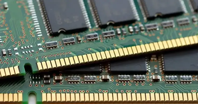
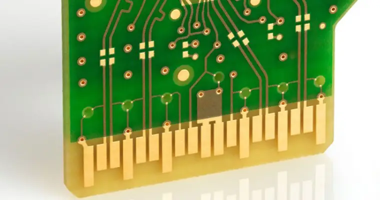
The gold fingers refer to the gold-plated connectors running along the edges of a printed circuit board. Their purpose is to allow a secondary PCB board to interface with the motherboard of a computer or device like a smartphone. In short, gold fingers on a PCB can be used as bridges to connect different chips and components to communicate through established protocols. They provide clear channels between computer chips and circuit boards to carry out instructions, which is especially critical for functions like WiFi, RAM, and processors.
There are two main surface treatment methods for gold fingers:
Electroless Nickel Immersion Gold (ENIG) – ENIG is widely used due to its solderability and surface flatness. However, it’s not suitable for high-frequency mating applications since its gold coating is thin (typically 2-5 u”) and soft, making it prone to wear from repeated insertions.
Hard Gold — Compared to ENIG, hard gold has thicker gold film (typically 30-50 u”), so it is more wear resistant and ideal for applications that require durability and repeated connections. The downside is the higher manufacturing cost.
Types of Gold Finger PCBs
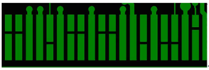
Gold fingers on printed circuit boards come in three main types:
- Regular gold fingers (also called flush gold fingers): These are rectangular solder padsof uniform length and width, neatly arranged along the edge of the board.

- Segmented PCB gold fingers(also called intermittent gold fingers): The solder pads here are rectangular but can be different lengths, located on the board edge. They have a disconnected section at the front.

- Long-short gold fingers (also called uneven gold fingers): These are rectangular pads of different lengths along the board’s edge, often referred to as long-short gold fingers or uneven gold fingers. You’ll often find this type used for connections in memory modules, USB drives, card readers, etc.
What Are PCB Gold Fingers Used For?
PCB gold fingers have a variety of common uses that enable connections between components in computers and other devices. Here are some of their most widespread applications:
Interconnection Points — Secondary PCBs connect to the main motherboard through female slots like PCI, ISA, or AGP. The gold fingers in these slots transmit signals between peripheral devices and cards and the computer itself. This is common in computers (memory and expansion card slots), servers, and industrial control systems.
Special Adapters — PCB gold finger connectors enable numerous performance add-ons for personal computers through perpendicular expansion cards that slot into the motherboard, delivering enhanced graphics processing and audio output. These are commonly found in gaming PCs and workstations that demand higher performance.
External Connections — Peripherals added to a computer station, like speakers, scanners and printers, plug into specific slots on the back of the tower. These ports connect to PCBs that then interface with the motherboard through gold fingers. In addition, automotive electronics, home entertainment setups all depend on gold finger connections for stable, and reliable performance.
PCB Gold Finger Beveling
PCB gold finger beveling refers to the process of cutting the circuit board edge at an angle to create a tapered profile along the gold fingers. The purpose of this procedure is to make it easy for the fingers to inserted into the matching slots and connectors.
PCB Gold Finger Plating and Beveling Process
Gold finger plating is done on the circuit boards after the application of solder mask but before the final surface treatment process. There are three stages of the process:
- Nickel plating: First, plating a nickel base layer onto the connecting edges of the fingers. This is done to establish a barrier layer that enhances the adhesion between the copper and the gold layer and prevents copper diffusion into the gold layer.
- Gold Plating: Next, hard gold is plated over the nickel layer. The gold is sometimes alloyed with cobalt in order to achieve increased hardness, decreased surface resistance and an extended life for the gold fingers even after multiple mating cycles.
- Beveling: The last step is beveling the edges of the gold fingers at an angle of 20°, 30°, or 45° based on the board thickness and connector requirements.
PCB Gold Finger Beveling Parameters at MOKO Technology
The table below outlines the standard chamfer parameters used at MOKO Technology:
| Angle(α) | PCB thickness(d) | Remaining thickness(s) | Chamfer depth(h) |
| 20° | 1.6mm | 0.5mm | 1.51mm |
| 2.0mm | 0.65mm | 1.85mm | |
| 2.4mm | 0.7mm | 2.34mm | |
| 30° | 1.6mm | 0.5mm | 0.95mm |
| 2.0mm | 0.65mm | 1.16mm | |
| 2.4mm | 0.7mm | 1.47mm | |
| 45° | 1.6mm | 0.5mm | 0.5mm |
| 2.0mm | 0.65mm | 0.65mm | |
| 2.4mm | 0.7mm | 0.7mm |
Design Rules of PCB Gold Fingers
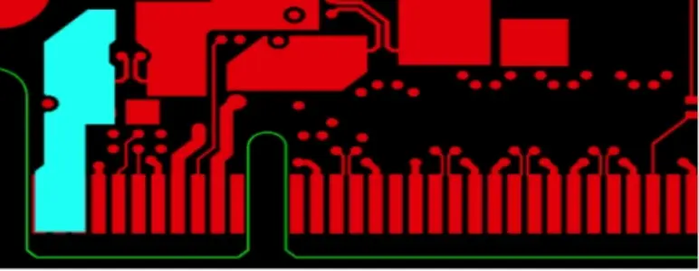
- Keep plated through holes away from the fingers by at least 1mm. Plated through holes require copper plating around the hole on all layers. This copper can flow onto the gold fingers during plating and cause contamination or plating thickness issues. Maintaining a 1mm keepout prevents this.
- Maintain spacing between the fingers and any solder mask or silkscreen printing. This prevents material from overflowing onto the fingers during application which can interfere with insertion.
- Orient the fingers on the side of the board opposite from the component center. This aids in insertion and alignment as it clears components on the bottom side.
- Do not place any SMD parts, plated through holes, or solder pads within 1mm of the fingers. This prevents interference with the interfacing connector.
- Remove all inner layer copper beneath the fingers, typically 3mm beyond the edge of the finger width. This prevents inner layer copper from being exposed during PCB beveling/chamfering which looks bad aesthetically.
- Limit the maximum finger length to around 40mm. Longer fingers are prone to damage during handling and insertion.
- Avoid soldermask or silkscreen printing in areas immediately adjacent to the fingers where material can overflow causing buildup issues.
- Design continuous openings in the solder mask around the fingers. This prevents the need for score lines or steel mesh.
Standards of Circuit Board Gold Fingers
PCB gold fingers need to meet strict quality and performance standards to ensure the reliable operation.The key aspects of printed circuit board gold finger standards include:
- Visual Quality: No scratch deeper than 0.1μm or longer than 1mm, no blistering, no oxidation and no foreign residues. Inspected at 20–50x magnification according to IPC-A-610 Class 2/3 standards.
- Plating Quality: Hard gold layer ≥0.8μm, nickel underlayer ≥ 5μm. Gold purity ≥99.9% and nickel purity ≥99.5%. Pull test to measure adhesion strength ≥0.5N/mm.
- Dimensional Accuracy – The length tolerance is ±0.1mm, the width tolerance is ±0.05mm, the pitch tolerance is ±0.03mm, and the chamfer angle is 45° ± 5°, and the chamfer length is 0.5~1mm.
- Electrical Performance — Initial contact resistance does not exceed 50mΩ, and does not exceed 100mΩ after 1,000 insertion cycles. The resistance variation must be ≤10% when using 1A current for 1 hour.
- Environmental Resistance — Withstand thermal cycling -40°C to 85°C for 50 cycles, pass salt spray test at 5% NaCl for 24-48 hours, and vibration testing at 10-2000Hz with no plating loss.
Conclusion
Gold fingers of printed circuit boards may be small in size; however, they serve a vital purpose in ensuring that electrical connections are made effectively among different devices, ranging from consumer electronics to automotive and industrial applications. Thus, it is important to know about the types of gold fingers, their uses, design rules, and standards.
At MOKO Technology, we’ve been producing printed circuit boards for almost 20 years. We are capable of manufacturing high-quality gold fingers on circuit boards. We follow industry standards closely to ensure the gold plating has the right hardness and adhesion. If you have any questions about our gold finger fabrication capabilities, please click here to contact us.