What Is a PCB Board?
A PCB board refers to a board that provides an electrical connection for different components by using wires and conductors and offers mechanical support for surface-mounted and socketed components as well.
It contains thin copper tracks, or traces, intricately etched into substrate material providing insulation, such as fiberglass or composite epoxy. The copper traces form the wiring between components on the PCB board. The PCB manufacturing process uses photolithography to accurately print the circuit onto the board. Once the PCB board is manufactured, electronic components can be soldered onto the copper pads to form a complete circuit. The PCB board provides the connections between these mounted components and integrates them into a functional electronic system.
While PCB boards can be found in nearly all electronic equipment today, the term specifically refers to the bare board without any components populated on it. When the components are soldered onto a printed circuit board, the resulting product is more precisely described as a printed circuit assembly (PCA) or printed circuit board assembly (PCBA).
Types of the PCB Board
Single-sided PCB Board
It refers to a PCB board made of a single-layer substrate with all its circuits and components mounted on only one side. Single-sided PCB boards are featured with a simple design and manufacturing process, high production efficiency, low cost, and a wide range of applications.
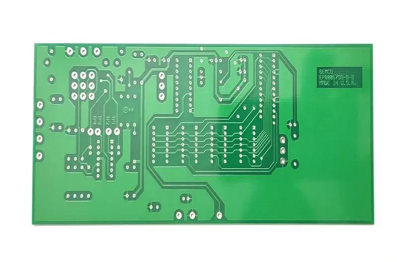
Double-sided PCB Board
True to its name, a double-sided PCB board refers to the board that is mounted electronic components on both sides of the substrate. And there are two methods to assemble components: SMT (surface mount technology) and THT (through-hole technology). It is usually applied for applications that are required with more complex circuits such as LED lighting, vending machines, industrial controls, and so on.
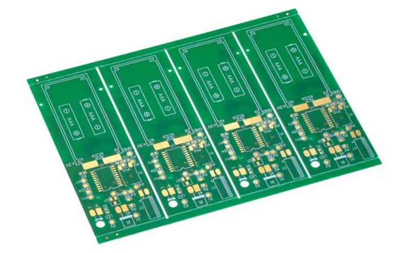
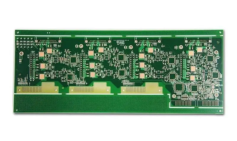
Multi-layer PCB Board
Multi-layer PCB boards consist of three or more layers of circuit boards, depending on the application and needs. This type of PCB gives designers way more flexibility for complex layouts, which is why you’ll find them in electrical powerhouses like medical devices, data storage systems, GPS tech, and other advanced applications. Having multiple conductive layers means components and traces can cross paths without shorting out, enabling far denser designs. So when you need a high-performing board to handle some serious electrical demands, multilayers are the way to go.
Rigid PCB Board
Rigid PCBs are a common type of PCB, which are made of strong substrate material. Their flexibility and bending are greatly reduced, thus the electronic components used for rigid PCBs have a longer lifespan.In addition, this kind of PCB board produces low electronic noise, so the use of rigid PCB board helps to reduce the negative impact on the environment to a certain extent. Rigid PCB board is mainly used in applications like satellites, automobiles and aerospace, etc.
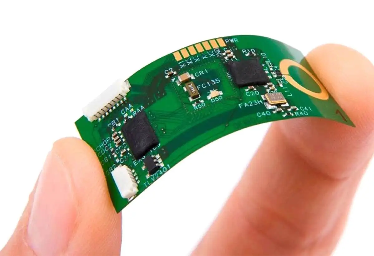
Flexible PCB Board
Unlike rigid PCBs, flexible printed circuit boards are made of materials that can bend easily, but they tend to be more expensive to manufacture. Flexible PCB boards have many advantages, the most prominent being their flexibility. They can be folded over edges or corners, while, due to their flexibility, a single flexible PCB can cover areas that might require multiple rigid PCBs. In addition, flexible PCBs require less assembly space and are suitable for applications where weight and space are important.
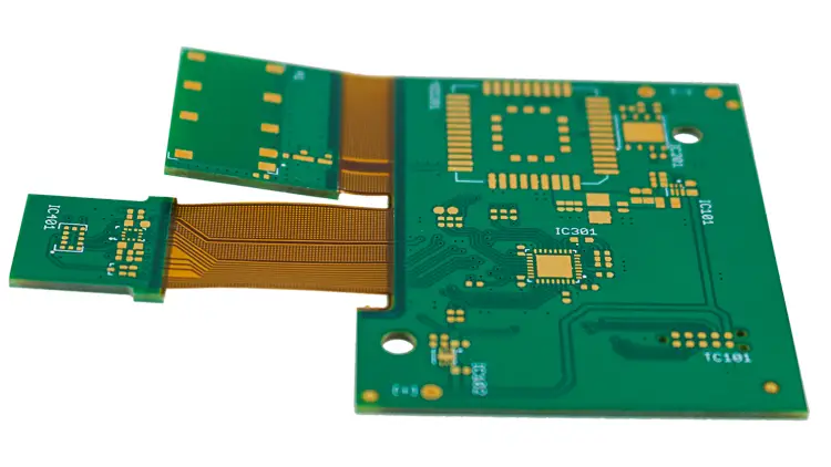
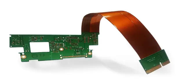
Rigid-Flex PCB
Rigid-flex circuits combine the advantages of rigid PCBs and flexible PCBs, and are implemented by connecting multiple layers of flexible PCBs to rigid PCB layers. Compared to rigid or flex boards, rigid-flex boards have fewer electronic components and do not require connectors, headers and contact crimps, resulting in a smaller overall PCB size and package weight. You’ll often find flexible rigid PCBs in things like mobile phones, digital cameras, and pacemakers.
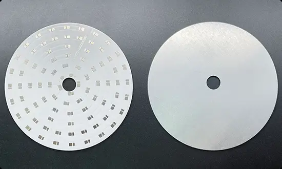
Aluminum-Backed PCB Board
Aluminum-Backed PCB refers to PCBs that use aluminum or copper substrates, while most PCBs are generally made of fiberglass. They have several advantages: First, they have better thermal efficiency, which makes them a perfect choice for some projects with more complex circuits, as they can easily dissipate heat from the circuit in time even after a long-term operation. Second, greater durability, aluminum PCB board has a longer lifespan compared to fiberglass. Third, they are harmless to the environment. Aluminum sheets are non-toxic and environmentally friendly, and easy to recycle.
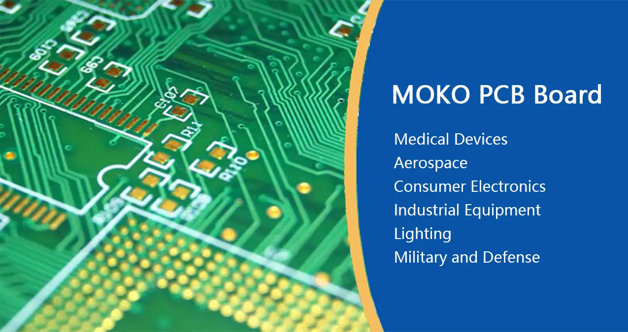
The Applications of PCB Board
Medical Devices
From pacemakers, tiny cameras used in minimally invasive surgery, to large medical equipment such as X-ray equipment and CAT scanners, PCB boards play an important role. For example, flexible and rigid-flex PCBs, which are small in size, light in weight and high in density, can be used to manufacture more compact and lighter medical devices, and for some complex medical devices, rigid-flex PCBs are a particularly ideal choice.
Aerospace
With the advancement of aerospace technology, the demand for PCB boards used in aircraft, satellites, drones and other avionics is also increasing. In these applications, PCBs that are small in size and support complex circuits are often used. Among them, the most widely used are rigid, flexible and rigid-flex PCBs, which are used in instrument panels, flight control, flight management and safety systems. Their small and lightweight design reduces overall equipment weight, which reduces fuel consumption requirements.
Consumer Electronics
We can find PCB boards in electronics commonly used in the home and office such as computers, smartphones, televisions, household appliances, entertainment systems, and so on. These products have high requirements about PCB boards including their reliability, weight and heat dissipation performances.
Industrial Equipment
Most of today’s industrial equipment is electronically controlled, resulting in an increasing demand for PCB boards across the industry. Equipment like manufacturing equipment, measuring equipment, power equipment, robots all requires PCB boards. Since industrial equipment usually operates in harsh environments, PCBs used in industrial environments must be durable enough to withstand chemical stimulation, physical shock, high temperatures, and other adverse factors.
Lighting
Due to their high energy efficiency and longer lifespan of light-emitting diodes, they are becoming more and more popular in different markets, which leads to the increasing usage of LED PCB boards, especially the aluminum-back PCB board with better heat dissipation compared to other types of PCB boards.
Military and Defense
Military and defense equipment is also inseparable from PCB boards, which are required for vehicles, computers, communications and monitoring equipment. PCBs used in this field must be very durable and reliable, and can withstand extreme temperature and weather conditions.
How to Manufacture a PCB Board?
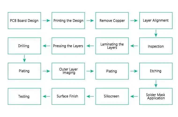
- Step 1 –PCB Board Design
Before the manufacturing, we need to make a PCB design first based on the project requirements. The design is normally completed by using computer software such as Altium Designer, OrCAD, Pads, etc. And when we finished the design, we need to convert it into the Gerber format that includes important information like drilling patterns, boreholes, component symbols.
- Step 2 – Printing the Design
We use a special printer called a plotter to print the PCB board design. The plotter is featured with high precision that can show details and layers of the circuit boards, which is very helpful for manufacturers to image the PCB boards. And there are two colors that would be shown in the film: clear ink and black ink. For inside layers, the clear ink represents the non-conductive areas and the black ink represents the conductive copper traces and circuits. While for outer layers, the meaning of them is opposite.
- Step 3- Remove Copper
To continue the manufacturing of PCB board, we must remove the extra copper in the inner layers of the board by using the copper solvent and the desired copper can remain intact. The amount of copper etch solvent used may vary, for instance, the large PCB board requires to use more copper and time.
- Step 4–Layer Alignment
In this step, the PCB board would move to the next step: layer alignment. Both inner and outer layers need to be aligned by using an optical punch machine which can drive a pin down through holes to align the layers of the printed circuit boards.
- Step 5 – Inspection
There is no possibility to correct errors of the inner layers if the layers are put together, thus, inspection is a very vital step. The automatic optical inspection machine would be utilized to ensure that there is no defect on the boards. By using a laser sensor, the machine would scan layers carefully and generate a digital image to compare with the original Gerber file. If there is any inconsistency found during the process, the machine would present the comparison so we can know more details.
- Step 6- Laminating the Layers
First, the layers would be fixed together by using metal clamps, and the prepreg layer is located on the alignment basin. Then the layer of substrate is covered on the prepreg before the copper foil layers are placed. And more sheets of prepreg would be covered on the top of the copper layer. Finally, the aluminum foil and copper press plate finish the stack.
- Step 7 – Pressing the Layers
To press these layers, pins need to be punched through layers to keep them aligned, then the pressing machines would apply heat and pressure to layers to melt the epoxy inside of the prepreg to fuse layers together.
- Step 8 – Drilling
Before drilling, we need to use X-ray machines to locate drill spots, then the computer-guided drill is applied to make holes in each layer. Once the drilling is finished, the extra copper wire on the edge of the panel will be removed by the contour tool.
- Step 9 – Plating
After drilling, the PCB board would be plated. We use the chemical deposition to fuse all layers together, and the board would be cleaned thoroughly by using other chemical solutions that would coat the surface of the panel with a thin layer (about 1 micron) of copper, which would go into the drilled holes.
- Step 10 – Outer Layer Imaging
In this step, we apply a layer of photoresist to the outside layer before imaging. During the process, we should notice that it should be down in a sterile room to isolate contaminants from the layer surface. Then we utilize the ultraviolet light to harden the photoresist, while any undesired photoresist would be removed.
- Step 11 – Plating
Just like what we did in step 9, we need to plate the panel with a thin copper layer. Then, the panel would be plated with thin tin. During this process, we can remove the unwanted copper and protect the copper of the outer layer from being etched off in the next step.
- Step 12 – Etching
By applying the chemical solution, we can remove unwanted copper in this step, while the desired copper that is guarded by tin can still remain. This step can establish the conducting areas and connections of the PCB boards.
- Step 13 – Solder Mask Application
Before the solder mask, both sides of the panel need to be cleaned. Then an epoxy solder mask ink would be applied to cover the panel. Then the ultraviolet light is applied to remove the unwanted solder mask, and the desired solder mask would be baked in an oven to cure.
- Step 14– Silkscreen
In this step, we would print critical information onto the board, which is a very important step. And once it is completed, the PCB board would move to the last coating and curing process.
- Step 15 – Surface Finish
According to different requirements, the PCB board can be plated with a solderable finish that can improve the quality of the solder.
- Step 16 – Testing
Before delivering the PCB board to customers, an electrical test on the board is required to test the functionality of PCBs and to confirm if they followed the original design.
Working with MOKO for Your PCB Board Projects
The design and production of the PCB board is a very complex process. To ensure the quality of the PCB, it is necessary to ensure the high-quality completion of each link, because the errors that happened in any link will lead to the failure of the whole PCB board. Therefore, it is very important to find a professional supplier.
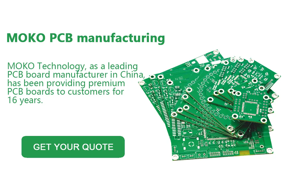
MOKO Technology, as a leading PCB board manufacturer in China, has been providing premium PCB boards to customers for 17 years. Our extensive experience makes us confident to handle kinds of PCB projects, more importantly, we have certification in ISO9001:2015, ISO14001, ISO13485, ROHS, BSCI and UL, thus, the quality of our PCB boards is guaranteed. The PCB board manufacturing daily capacity at MOKO reaches 1000 square meters, and PCB assembly can reach 100,000,000 units per month, making sure that we can deliver PCBs to you with a short turnaround time. If you are looking for a PCB board manufacturing that can always meet your requirements both in quality and price, MOKO is your go-to choice.