8 Common PCB Surface Finishes: How to Choose the Right One?
PCB surface finish is a coating or treatment applied to the exposed copper traces and pads of a circuit board. It plays a critical role in PCB functionality and lifespan.


PCB surface finish is a coating or treatment applied to the exposed copper traces and pads of a circuit board. It plays a critical role in PCB functionality and lifespan.
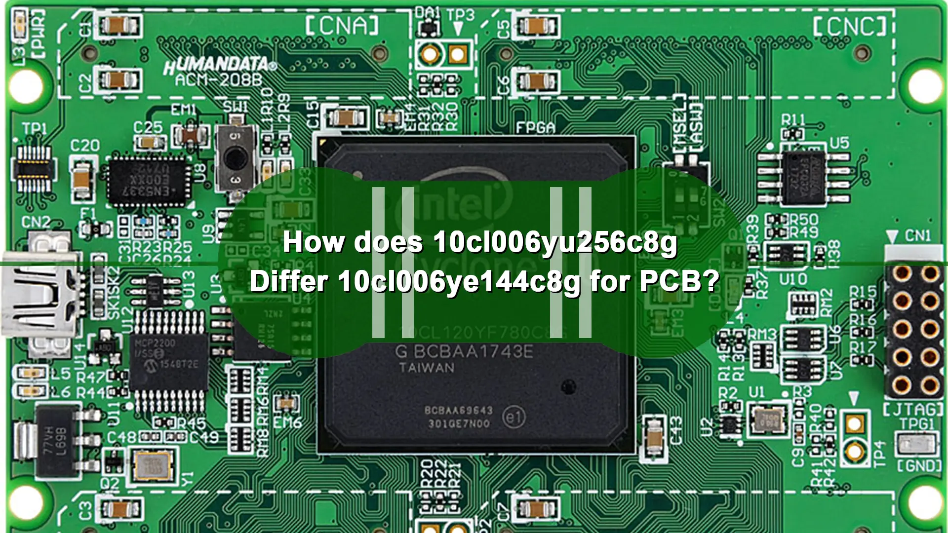
10cl006yu256c8g is a common chip applied in PCB, with always another backup choice, 10cl006ye144c8g. So how do we make a choice between 10cl006yu256c8g and 10cl006ye144c8g during PCB assembly? Let’s dive into
Bluetooth is everywhere these days! You can find it in smartphones, headphones, speakers – pretty much any gadget that connects wirelessly likely uses Bluetooth. So when building a new electronic

PCB trace width specifically refers to the width of copper traces that carry vital signals and power across the printed circuit board. Determining appropriate trace widths is an important PCB design
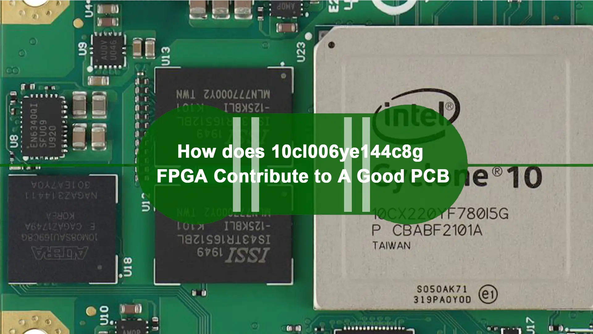
The recent decade witnessed the emergence and booming of AI robots, medical devices, 5g technology, and the semi-auto vehicle industry. Accordingly, 10cl006ye144c8g FPGA, as a high-tech PCB assembly, must play

The growing demand for advanced electronics drives innovations in circuit board capabilities and performance. Circuit designers now routinely work with faster signal speeds. High-speed signals, once an occasional challenge, are
As electronics shrank in size and cost, consumer product manufacturers pressed for similarly miniature and affordable components. This drive catalyzed the development of the printed circuit board. The PCB utilizes
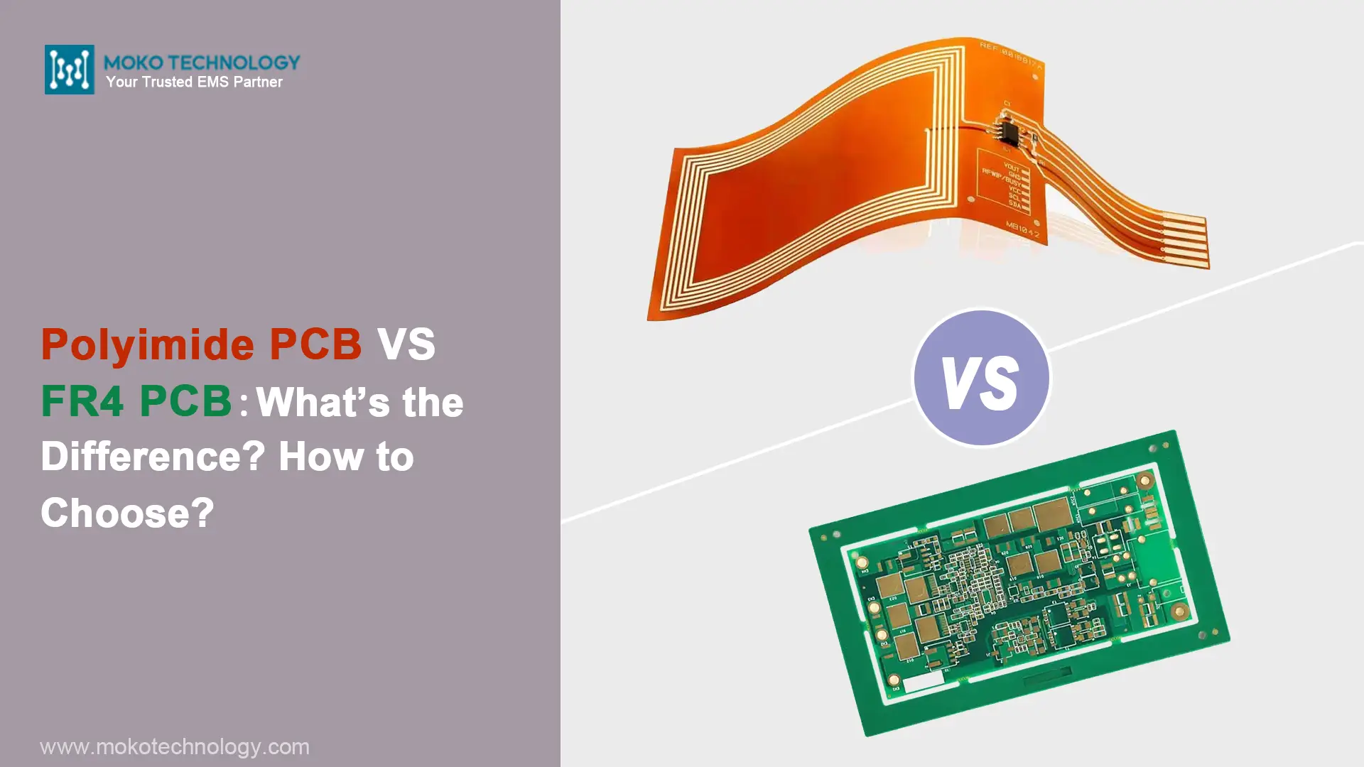
Polyimide PCB and FR4 PCB are two of the most prevalent used PCB types. Though both are polymer substrates well-suited for PCBs, Polyimide and FR4 each possess their own distinct characteristics
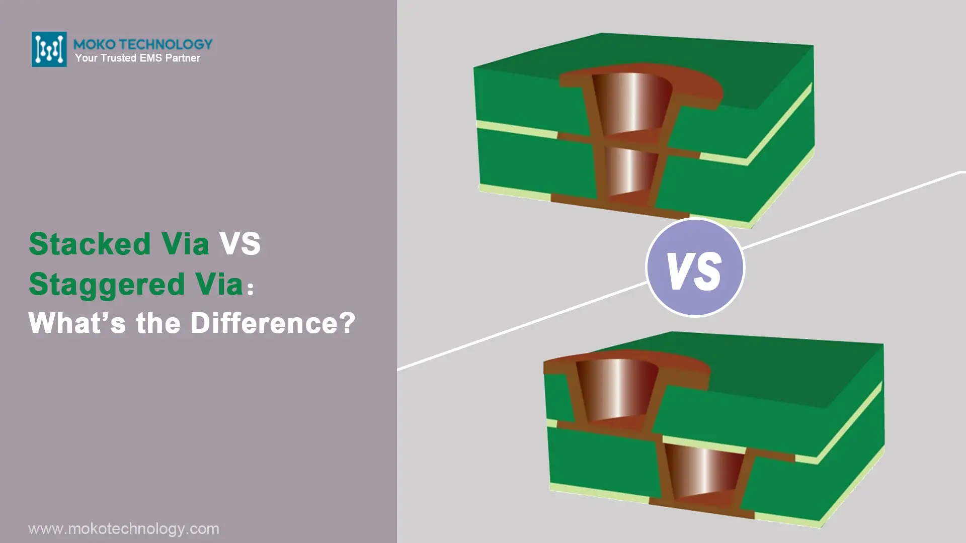
A common question when designing complex printed circuit boards for advanced electronics is whether to use stacked or staggered vias to route connections between layers. Vias act as conductive pathways