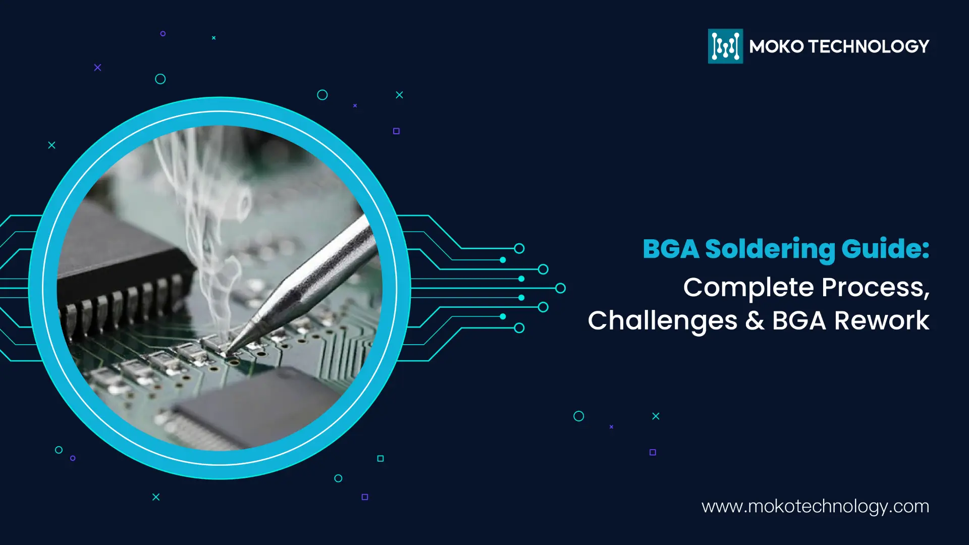
BGA soldering is one of the most critical processes in electronics manufacturing today, especially as Ball Grid Array (BGA) technology is poised to continue using higher density chip technology and better performance in a smaller footprint. Working with BGAs comes with their own special challenges, which requires precise techniques and specialized knowledge. In this comprehensive guide, we’ll walk you through everything you need to know about BGA soldering, from basic concepts to complete process involved and BGA reworking.
What Is BGA ?
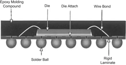
Ball Grid Array is a distinct surface-mount packaging technology that differs from traditional packages, which typically use perimeter leads. BGA is featuring leads of ball shape which are being distributed in arrays at the package’s bottom. And the ball array is actually getting its name because it is a metal or alloy ball array that is arranged in a grid. This innovative design allows for efficient use of space and better thermal performance, making BGA an ideal choice for modern, high-density circuit board applications.
How to Solder BGA Components on a PCB?
First, solder paste is applied to the PCB pads where the BGA solder balls will make contact. The solder paste is usually dispensed through a stencil or screen printing process to ensure accurate and repeatable application.
Then, the BGA component is precisely positioned and temporarily tacked in place on the PCB. This is done using pick-and-place equipment with high precision X-Y motion control and optical alignment systems. Proper alignment is critical.
Then, the PCBA is sent through a reflow oven with a defined temperature profile. The solder paste melts, the BGA’s solder balls melt and fuse with the PCB pads, forming the solder joints. The profile must be hot enough to reflow the solder without damaging components.
Last, after cooling, the solder joints are inspected for proper formation with no defects. Any rework needed is completed using specialized BGA rework equipment and procedures.
Common BGA Soldering Challenges and Solutions
- Precision Alignment Challenges
The size of connection pitches is as small as 0.5mm, making the BGA packages placement a big challenge. Ensuring the precise alignment is crucial as even slight misalignment can result in the connection failure or shorts between adjacent balls. To solve this problem,advanced optical alignment systems and automated placement equipment are needed.
- Thermal Management
The other challenge is in getting the heat evenly throughout the entire component and substrate. Uneven heating can cause PCB warping, incomplete solder melting, or inconsistent joint formation. Developing of the reflow profiles with controlled preheating phase, precise temperature ramping and monitored cooling cycles is required for successful thermal management.
- Inspection Difficulties
Traditional visual inspection methods are unable to be used for BGA connections as they stay hidden under the package. Advanced inspection techniques are needed to verify assembly quality, among them, X-ray inspection is regarded as the most reliable methods that can penetrate the package.
- Solder Joint Quality Control
In BGA assembly, the formation of consistent and reliable solder joints is a big challenge. Connection failures can occur with inconsistent solder paste volume, improper wetting, and so on. To address these challenges, comprehensive quality control measures including exact paste application control, optimized stencil design, and well controlled atmospheric conditions of reflow have to be executed.
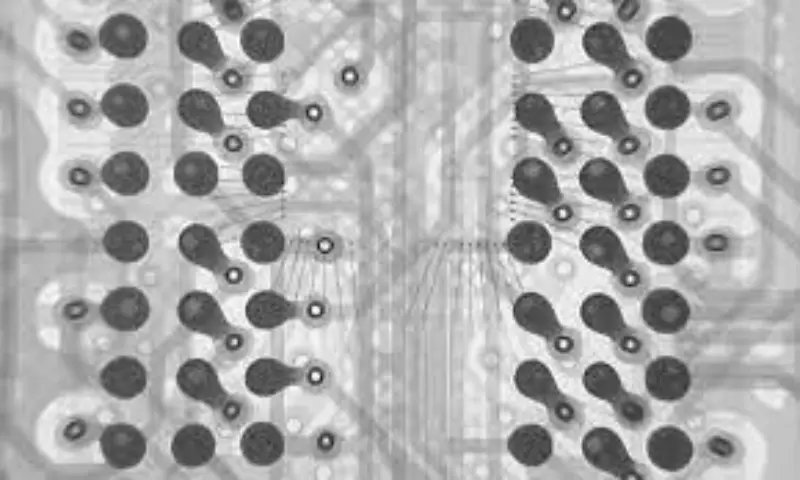
BGA Soldering Joints Inspection Methods
It’s important to inspect the connections between BGA components and PCBs. Since direct visual observation of solder joints is nearly impossible, multiple inspection methods are employed for comprehensive analysis:
1.Electrical Testing
This testing method allows us to test electric properties of the board. It’s valuable in detecting defects, but cannot determine where they are. It is usually used in conjunction with other inspection techniques.
2. Optical Inspection
The advanced endoscope technology allows technicians to examine the outer rows of BGA connections. This method can evaluate solder joint shape and surface texture as well as defects, including shorts and debris, and cold solder joints.
3. X-Ray Inspection
X-ray inspection is the most sophisticated method of which detailed images of the solder patterns from a variety of angles are available. Dense areas like solder joints appear darker, creating a visible grid pattern. It is an excellent technique for detecting solder bridges, popcorning, and over applied areas, but is poor at finding opens.
BGA Rework Process : Step-by-Step Explained
When a ball grid array component is found to be defective, a rework process is required to remove and replace it. Below are the key steps involved:
Preheat the PCB: Start by preheating the PCB to prevent thermal shock and reduce the risk of warping.
Apply Controlled Heat: Use a hot air or infrared rework station to carefully heat the BGA component, softening the solder balls.
Remove the BGA Component: Once the solder is softened, gently lift the BGA component from the PCB.
Clean the Pads: Remove residual solder from the PCB pads using a solder wick and flux, ensuring a clean surface for the new component.
Reball or Replace: Prepare a new BGA component with fresh solder balls or use a reballing stencil if reusing the existing component.
Align the Component: Use an alignment tool to accurately position the BGA component onto the cleaned pads.
Reflow Soldering: Secure the BGA with reflow soldering to establish a strong bond and reliable electrical connections.
Inspect the Joints: Conduct an X-ray or Automated Optical Inspection (AOI) to verify proper alignment and solder joint quality.
Additional Tips for Successful BGA Rework:
- Match solder alloys to ensure joint compatibility
- Balance adhesive tack strength for positioning adjustments
- Follow prescribed thermal profiles closely
- Use the minimum required airflow setting
- Raise BGA slowly post-reflow, avoiding scrubbing
- Select nozzle size matching the component
Final Thoughts
Implementing robust BGA soldering, inspection, and rework processes requires investments in specialized techniques, equipment, and operator training. But the benefits of higher density BGA packaging make this effort worthwhile for quality and performance. With expertise in precision printing, accurate placement, profiled reflow, x-ray inspection, and controlled rework, manufacturers like MOKO Technology enable customers to take full advantage of BGAs across critical applications. As a leading PCB assembly provider with nearly 20 years of experience, MOKO specializes in advanced Ball Grid Array soldering technology. Contact us today to discuss your particular BGA project and assembly requirements.