What is a Gerber File?
Gerber is a file format that we frequently use in the PCB industry. We use a Gerber file to describe the various elements and constituents of a printed circuit board. So, this includes things like legend layers, the metal we are going to use, conductor layers, wiring pads, and the solder mask layers. The Gerber format was developed and mainstreamed by a company known as Gerber and hence from there came the name.
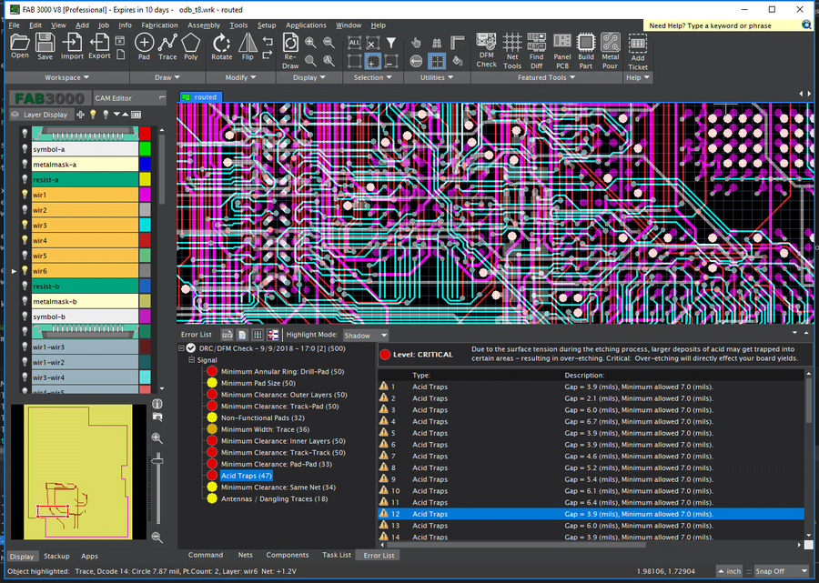
We design PCBs by using a special set of tools. So, these tools mainly include CAD (Computer Aided Design) and EDA (Electronic Design Automation). These tools help us in generating fundamental PCB fabrication data. We then commence the manufacturing of PCBs based on this data. If a customer gives a PCB design file to a manufacturer without including the Gerber file then the manufacturer will face a lot of difficulties. This is because the Gerber file extensions are empirical to PCB manufacturing as it serves as a set of guidelines and references. Manufacturers rely on the PCB Gerber viewer for describing and understanding the designing parameters of various modules of a circuit board. Hence, we can utilize a Gerber file for both PCB fabrication and PCB assembly.
The importance of a Gerber File
PCB designs are becoming more complex and demanding the use of small components in compact designs. As a result, the vector photoplotter tools previously used are no longer adequate. They could only trace single-layered designs and component locations. However, with the advent of PCB Gerber files, even designs with more than 20 layers can be traced accurately. This makes Gerber files crucial for the PCB manufacturing and fabrication industry as they allow for tracing of every layer of construction, including solder paste layers and component locations.
Before, vector plotters necessitated a concentrated beam of light that passed through an opening to reveal the design on film. However, these photo plotters are no longer appropriate for the intricate, high-density, and compact PCB designs of today. Laser plotters, which are ideal for mounting high-density components on PCBs, are employed by Gerber files to track the position of components.
Gerber files for PCBs offer a time-saving advantage. When working with a large PCB that has many trace lines and component locations, using a Photo Plotter tool can be a time-consuming task. Fortunately, the use of Gerber files drastically reduces this process to just a few minutes, thanks to the efficiency of a laser plotter.
If the need arises to return to traditional photo plotters, retrieving information from Gerber files is a straightforward process. Converting Gerber coordinates into a raster file with a laser plotter helps to maintain information traces for an extended period. These impressive capabilities highlight the crucial role that PCB Gerber files play in the fabrication process. Moreover, their significance is further amplified by additional features that are intrinsic to their usage.
Different versions of Gerber Files
Gerber file format is always evolving so it has had many versions in the past. However, today we mainly use three popular versions of the Gerber file.
1) Gerber X2
This is the latest free Gerber viewer format. The best thing about this version is that it supports stack up data. Additionally, it also contains a number of advanced attributes.
2) RS-274-X
This version of the PCB Gerber file has the most expanded functionality. So, we widely use this version in routine PCB file viewer online manufacturing operations.
3) RS-274-D
This version of the online Gerber viewer format is the oldest one and most conventional PCB manufacturers still use it. However, the other two versions are gradually replacing this version.
Gerber Files types and format
1) pcbname.GTL
We use this file type to store data relating to the top copper layer.
2) pcbname.GTS
We frequently use this file type to store data relevant to the top solder mask layer.
3) pcbname.GTO
We often use this type of file in our routine PCB manufacturing operations to store data relevant to the top silkscreen.
4) pcbname.GBL
Most PCB manufacturers use this type of file in their setups to store information and data relevant to the bottom copper layer.
5) pcbname.GBS
This type of format is most suitable for storing information and details about the bottom solder mask layer.
6) pcbname.GBO
This format is ideal for keeping a record of information relevant to the bottom silkscreen.
7) pcbname.TXT
We mostly use this file type or format for maintaining a record of the drilling information. This mainly involves data relevant to holes and other features that we are going to drill in our PCB boards.
8) pcbname.GML/GKO
This file format is most suitable for storing information relevant to the outline of the PCB board.
9) pcbname.GL2
We use this type of file only in multilayer PCB boards. It gives us information relevant to the second inner layer.
10) pcbname.GL3
This type of file is also reserved only for multilayer PCB boards. We use it for storing information relevant to the third inner layer.
How to generate a Gerber file from Eagle?
Autodesk Eagle is a very handy tool for PCB design and layout. It has scripting features that allow us to automate the electronic design process. Once you complete the design of your PCB board in Autodesk Eagle, the next step is to generate a Gerber file. This is because you will have to send this Gerber file example along with your other design files to your PCB manufacturer. One of the best things about Autodesk Eagle is that it includes a very intuitive CAM processor. This module allows us to import any CAM file and then immediately generate any kind of file that you may need for your PCB board. So, you can use this functionality to generate the required Gerber file.
1) Open the CAM processor
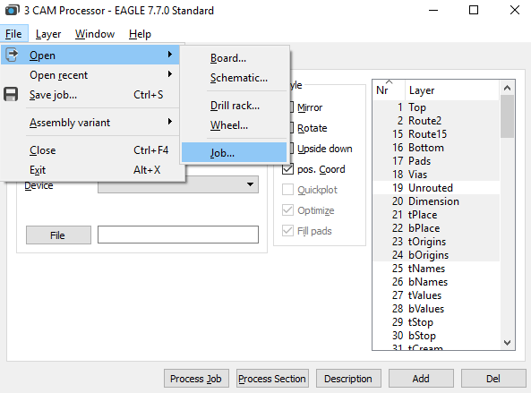
You will first have to import and open the PCB layout file in Autodesk Eagle. The PCB layout file has a (.brd) extension. So, for opening it you can click the CAM button. Alternatively, you can do this by first clicking on File and then navigating to the CAM processor. Doing this will immediately open the CAM processor that we are going to use for generating the Gerber files.
2) Navigate to Job
The next step is navigating to the job. You can do this by clicking on File and then clicking on open. Then toggle the job button.
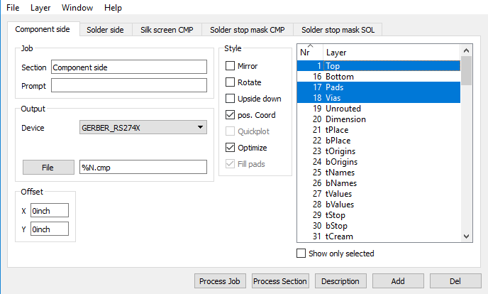
2) Open the gerb274x.cam file
You will have to first navigate to the default CAM folder of your Autodesk Eagle. So, from there you can choose the gerb274x.cam file. Once you have done that, you can select open.
3) Add a second silkscreen
If you browse through the tabs in Autodesk Eagle then you will observe that we do not have any file for the bottom silkscreen layer. This is because, in the case of simple PCB boards, we usually place the silkscreen only on the top layer. However, if you have a complex PCB and you want to add an additional silkscreen on the bottom layer, then you can do that as well.
- First of all, you will have to click on Add.
- Then you will have to change the section. You can use any relevant term such as “Silk Screen Bottom”
- After that, you will have to change the file to “%N.pls”
- Then you will have to deselect all the layers
- Then select these layers: 26 “bNames, 20 “Dimension, and 22 “bPlace”
4) Create a Gerber File
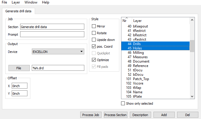
You can now finally create your required Gerber file. For this purpose, you will have to click the Process Job button. Then you will see that your required Gerber file is generated in the project folder of your Eagle control panel.
5) Sending the Gerber File to MOKO Technology
Once you have generated the Gerber files, you will have to send them to MOKO Technology so that we can start processing your order. For this purpose, you will have to put together all of your Gerber files and zip them in a single folder. Then you can upload this zip file to the order page of MOKO Technology. This will allow us to receive the Gerber files along with your order specifications. Hence, we will start working on it right away.
Common mistakes of Gerber file from eagle and how to solve it
1) Missing drill files
We need these files for determining the location and size of the holes that we are about to drill in a PCB board. If you forget to include these files then your PCB manufacturer can face a significant amount of difficulty.
2) Missing solder mask layers
If your PCB board has two or more layers then the files must have two solder mask layers. One is for the top layer and the other is for the bottom layer.
3) Missing or double outlines
One of the most common mistakes is that people often generate files that lack outlines. These outlines are important for identifying where to cut the PCB boards. Sometimes people mistakenly generate files where they include two or more boxes around the PCB board. In both of these scenarios, the PCB manufacturer can face severe problems.
4) PCB size mismatch
Often the dimensions of the PCB board entered in the order do not complement the dimensions entered in the Gerber file. You should avoid so that we can prevent any significant delays in PCB manufacturing.
5) Placement of Drill holes cut into the tracing
Sometimes people mistakenly place the drill holes in such a way that they interfere with the circuit tracing. On top of that, they forget to reroute the tracing around the hole. You should avoid this so that the functionality of the PCB board is not damaged.
6) Plated and non-plated holes are not clearly defined in Gerber File
Sometimes people lack a fundamental understanding of how the Gerber PCB software differentiates the NPTH from the PTH. In Autodesk Eagle, you can make the NPTH by using the hole tool. On the other hand, you have to use the Via tool for making the PTH.