Ball Grid Array (BGA) is one of the most popular packaging technologies nowadays. It is characterized by high pin count, small size, and good electrical performance. However, this technology also brings a major challenge: soldering quality inspection. Normally, we apply X-ray inspections for detecting BGA soldering problems and in this process, we have come across some common BGA soldering issues. In this article, they will be discussed one by one with regard to their causes; and more importantly, how to avoid them.
6 Common BGA Soldering Issues
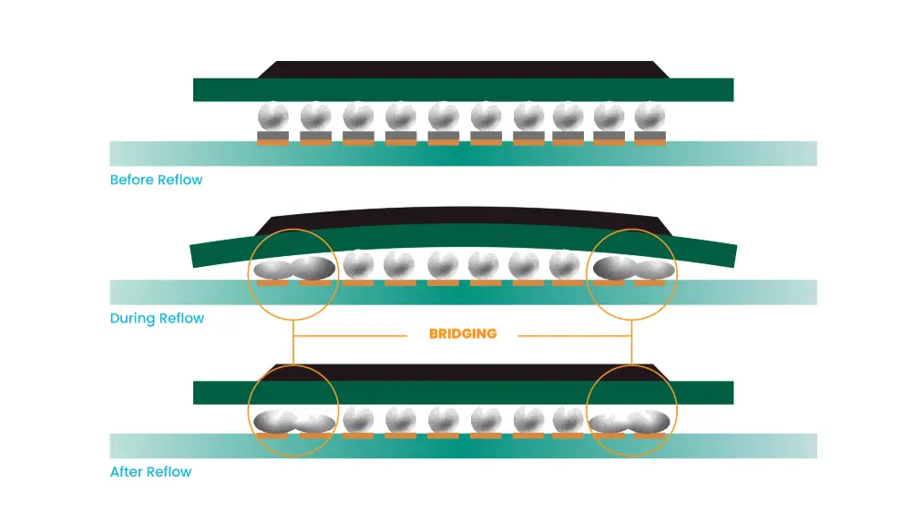
Solder Ball Bridging
Solder ball bridging is the situation whereby neighboring solder balls are connected together making a short circuit unintended. It is one of the problems that often occur and at the same time cause a lot of trouble during the assembly of BGA. The main causes of solder ball bridging include a rich supply of solder paste, wrong solder paste printing methods, improper positioning of components, and improper profiles during the process of reflowing.
Missing Solder Balls
Missing solder balls refer to the unintended absence or displacement of solder balls from a BGA package, which causes improper electrical connection and even power failure. This defect is easy to identify and is more apparent during the X-ray inspection of the BGA array. Possible causes for missing solder balls are thermal fatigue, the solder or other materials used being of low quality, improper placement of the balls, and solder balls flowing through the vias of the printed circuit board.
Head-in-Pillow Defect
Head-in-pillow is a kind of partial connection issue where the solder ball does not fully bond with the PCB pad, appearing like a head resting on a pillow in a cross-sectional view. This defect is generally attributed to the warpage of the BGA packager or PCB, oxidation of solder balls or pads, reflow temperature or time, or both.

Voids in Solder Joints
Another common BGA soldering issue is solder joint voids, which refer to air pockets or cavities within the solder joint, which, when large, pose a reliability threat to the joint. Even though some degree of voiding is deemed permissible, it presents a concern where it goes beyond the allowed limits. Reasons causing such issues include outgassing from the PCB or other parts, trapped flux, and/or an incorrect profile in the use of the reflow process.
Solder Ball Collapse
Solder ball collapse is one of the typical BGA soldering issues that make the distance between the BGA and the PCB to be smaller than is necessary. This can cause possible short-circuiting and mechanical lofting. The main factors that may lead to the solder balls’ collapse are excessive temperature or time for the reflow, the wrong quantity of the solder paste used, and the lack of support in the process of reflow.
Solder Ball Shift
Solder ball shift is the circumstance whereby BGA solder balls tilt in a definite direction, which results in incomplete alignment between the balls and the PCB pads. While this flaw does not impact electrical performance, as far as we are aware, it can potentially weaken soldering stability. Solder ball shift could be due to misalignment at a placement operation, and solder ball movement due to moisture; inadequate control of thermal expansion and contraction minute movement; the BGA part quality; and pad layout and dimension which may not have been well designed and matched during the design stage.
Suggestions to Avoid BGA Soldering Defects
- Ensure the solder paste you are using is fresh, the paste should be properly mixed, the application should be proper and the components placed properly.
- For plastic-encapsulated PBGA, it is recommended to dry at 100°C for 6-8 hours before soldering; nitrogen is even preferred.
- The reflow temperature profile is another important thing. When changing the temperature, make sure that it increases and decreases gradually, allowing the components to heat uniformly, particularly during the soldering process. In the soldering area, all solder joints should be fully melted. If the temperature is not sufficient, cold solder jointsmay occur, which would result in rough surfaces of the joint or incomplete fusion during the second collapse stage. This can create cracks between the solder paste deposited on the surface of the PCB and the solder on the component, producing poor or ‘cold’ solder joints.
- Apply an appropriate amount of solder paste. The viscosity of the solder paste helps temporarily fix the components and prevents the formation of solder bridges during the melting stage. In the case of BGA stencils, the aperture size for the solder joints is usually between 70-80% of the pad size and the thickness of the stencil is normally about 0.15mm (6mil).
- All pads on the PCB should be designed in the same size. If there are some processes requiring design under pads, the appropriate PCB manufacturer should be selected. The pad positions should be drilled properly, and the pads should not be enlarged in any way. This is because vias cannot be drilled too small, leading to the amount and height of solder after soldering large and small pads. As a result, weak or open connections could occur.
- Furthermore, during the PCB manufacturing process, we need to note the solder mask issue. Before BGA soldering, ensure that the solder mask surrounding the pads is qualified and that a barrier film is applied on the vias.
Final Thoughts
In this article, we list some typical BGA soldering issues and give some suggestions to avoid them. By implementing these measures, manufacturers can significantly reduce BGA soldering defects and improve overall product reliability. As the electronics industry continues to evolve, addressing these BGA soldering issues remains a critical aspect of quality control and product development.