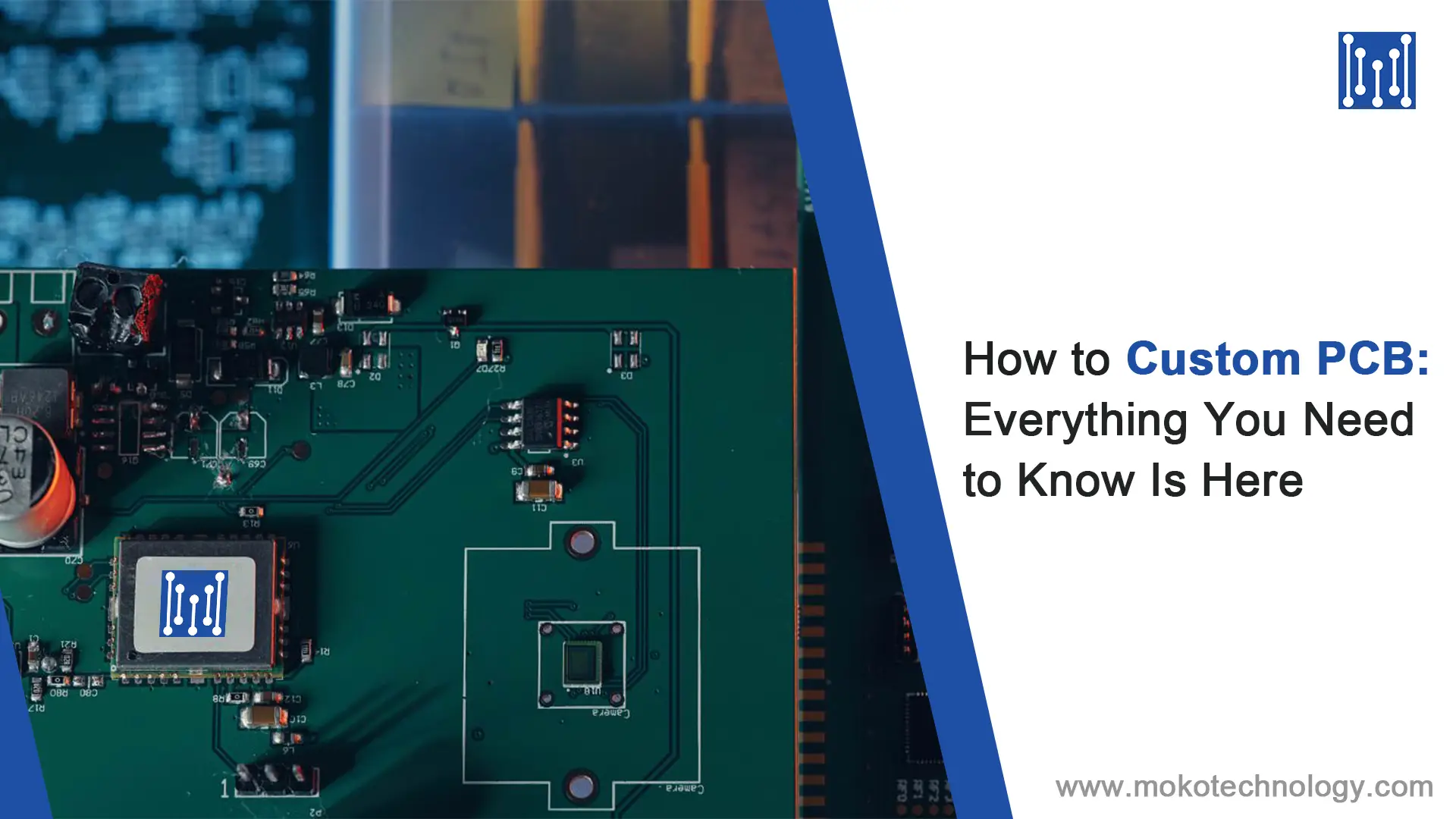
A custom PCB is a circuit board that is designed and manufactured according to exact specifications for a specific application, rather than using an off-the-shelf or standardized board. With over 90% of electronic devices using custom designed PCBs as their core component, it’s no wonder that custom PCB fabrication has become a critical service for supporting today’s complex and innovative electronic products. Whether you need a simple single-sided board or a multilayer beast with thousands of components, a custom PCB provides the perfect foundation.
This blog covers everything on custom PCBs. We’ll look at the pros and cons of going custom, the cost of custom PCB, and walk through the custom PCB fabrication process step-by-step.
Pros and Cons of Custom Circuit Board
Pros:
Tailored to Specific Needs: Custom circuit boards are designed to meet specific requirements, ensuring they are perfectly suited for a particular application.
Optimized Performance: Custom boards can be optimized for performance, leading to enhanced speed, efficiency, and overall functionality.
Space Efficiency: Custom designs can integrate multiple functions into a single board, saving space in the final product.
Cost Efficiency in Bulk: While initial setup costs can be high, custom boards can be cost-effective in large production runs due to reduced material waste and optimized manufacturing processes.
Improved Reliability: Custom boards can be engineered for specific environmental conditions, leading to increased reliability and durability.
Cons:
High Initial Costs: Designing and prototyping custom circuit boards can be expensive, especially for small production runs or individual projects.
Complexity: Custom designs require a deep understanding of electronics and may involve complex engineering challenges, requiring skilled professionals.
Time-Consuming: The design and testing phases of custom circuit boards can be time-consuming, leading to delays in product development timelines.
Limited Support: Off-the-shelf components often come with extensive documentation and support, which might be limited for custom-designed boards.
Lack of Standardization: Custom boards might not adhere to industry standards, making it challenging to find compatible components or troubleshoot issues.
How Much Does a Custom PCB Board Cost?
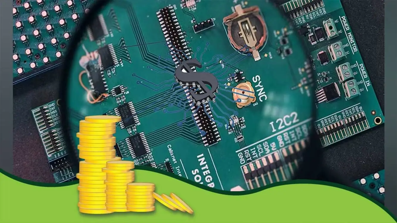
Custom PCB prices vary widely depending on design complexity, materials, layer count, and manufacturing methods. More complex circuits, high-end materials, extra layers, and special processes like HDI all increase costs. Custom PCB costs often fall between $10-$50 for simple designs. More complex boards with advanced features can cost hundreds per unit. Manufacturing in bulk or placing larger orders generally leads to a reduction in the cost per unit. But the exact custom cost is decided by specific requirements, to know the actual price, you should consult PCB manufacturers and provide them with detailed specifications to get an accurate cost estimate for your custom PCB board, including:
- The complete Gerber files
- Board Size
- Number of Layers
- Turn time
- Required quantities
- Materials requirement
- Finish requirements
- Panelization requirements
- Assembly requirements (including turnkey)
How to Custom PCB Boards-Step by Step
- Component selection and requirement analysis
The first step is to assess the intricate requirements of your PCB board. This includes choosing appropriate components like the power supply and processor. You’ll need to create a blueprint of all these requirements. Check out our other blog to get more knowledge about PCB components: Circuit Board Components: A Comprehensive Guide
- Design the PCB
Next, design the PCB layout with the help of custom PCB design software. The typical output of the software is a PCB schematic Gerber file, which encodes information like drill drawing, tracking layers, and component annotation, among other parameters.
- DFM checking
The next step is to run a Design for Manufacture (DFM) check before you can begin circuit board fabrication. This ensures that the design has no discrepancies.
- Print the inner layers
This involves cutting, cleaning, and drying the epoxy substrate before placing the film you formed in the last step on top of your panel. Lastly, UV-treat the panel.
- Etching the unwanted copper
An alkaline solution is used to wash away any unhardened part of the copper layer, ensuring that the required copper layer is intact.
- Punching the register for layer alignment
This involves optically punching the different layers for registration hole creation and ensuring that there is alignment.
- Automated optical inspection
In this step, you will have to use a laser sensor to scan the layers while looking for discrepancies between the Gerber files and the outcome.
- Layer up and bond
Involves bonding together the PCB panel layers with an aluminum press plate.
- Drilling
The next step is to drill holes into the PCB stack, allowing the electrical components’ placement and interconnection.
Further reading: PCB Drilling: Everything You Need to Know Is Here
- Copper deposition and platting
To cover the non-conductive materials and bond the panels, you will need to cover the entire panel with a fresh copper layer.
- Outer layer imaging and copper etching
Involves applying a photoresist material over the outer copper layer and imaging it.
- Solder mask application
The board is cleaned before applying the solder mask, which protects the board from copper corrosion, damage, and oxidation.
- Gold/silver surface finish and silkscreen
To protect the copper and solder components to the pads, you will need to plate the PCB with gold or silver. Next is to proceed with profiling or silk screening, which involves printing out critical details onto the board, such as the company name, debugging points, component numbers, and custom PCB manufacturer ID.
- Electrical testing
Probe testers are used to perform open and short circuit tests on your board, which ensures functional reliability. Durability tests follow this.
Our Capabilities and Services for Custom PCB Fabrication
Manufacturing Different PCB Types
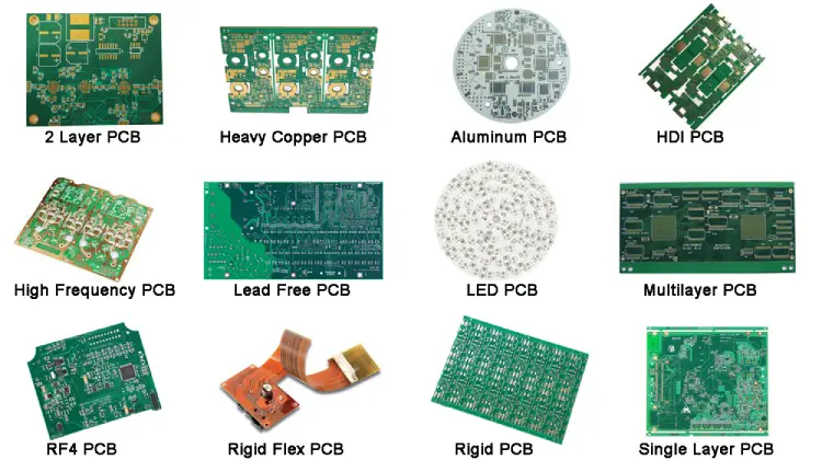
MOKO Technology, as a leading custom PCB manufacturer, is able to fabricate a wide array of PCBs, including:
- High-frequency PCB
- Heavy copper PCB
- LED PCB
- RF4 PCB
- Microware PCB
- Rigid PCB
- Carbon ink PCB
- Single-sided PCB
- Double-sided PCB
- Multilayer PCB
- Halogen-free PCB
- Lead-free PCB
- Standard PCB
- Aluminum PCB
- HDI PCB
- Rigid-flex PCB
- High TG PCB
Custom PCB Solutions We Offer
- Prototype PCB
We can complete over 700 PCB prototypes in less than a week for your testing or presentation. With our updated high-quality equipment and quick fabrication abilities, we’re more than certain to meet your simple or complex PCB prototypes needs in no time.
- Circuit Board Design
We provide unique custom design services to suit your specifications and applications through our comprehensive process that includes; preliminary design, prototype development, manufacturing integration, and finally, production.
- PCB mass production
MOKO’s PCB factory is equipped with advanced equipment and experienced operators, which allows us to complete customer orders within the fastest turnaround time, from small batches to large batches.
- PCB assembly
At our manufacturing facility, we utilize a range of advanced PCB assembly techniques to meet the unique requirements of each customer’s project, including SMT, THT and Mixed PCB assembly, and BGA PCB assembly.
- ERP system
Our ERP system guarantees cost-efficient manufacturing of PCBs through auto-scheduling, stable material supply, capacity planning, and real-time monitoring to boost production capabilities.
Our Capabilities
| Parameter | Description |
| Base material | FR4, Halogen Free Material, Rogers HF material, High TG FR4, CEM-3, |
| Number of layers | 2-36 layers |
| maximum PCB thickness | 3.2 mm, special: 6.50 mm |
| Min PCB thickness | 0.1 mm |
| Max board size in mm | 480 x 580, special: 584.2 x 1041.4 |
| Copper scratches | 18 or 35 µm, M: 9 µm, 210 µm, all the way up to max. 350 µm |
| Min track width in MIL | 3/3 or 4/4 or 5/5 or 6/6 or 7/7 |
| Min hole diameter | 0.2mm, 0.3m, and so on |
| Surface finish | Gold, Tin, HASL with and without Lead, Silver |
| conductor tracks intervals | 100 µm |
| Solder-stop-masks | Removable solder mask, a UV-hardened solder resist, and a Dry-film mask |
| Design options | Bond areas, SMD |
| Marking printing | It can be done in all catchy colors |
| Mechanical machining | scratch, mill |
| Other finishing options | hole metallization with silver, carbon coating |
MOKO Technology- A Reliable Custom PCB Manufacturer
High-quality raw materials: our strict supplier selection policy, standardized procurement process, and traceable source of raw materials ensure that we can work with quality raw materials.
Advanced equipment: Our investments in advanced manufacturing tools streamline production and deliver exceptional quality. This equipment helps slash production lead times for a faster time to market and lower custom PCB costs.
Strong manufacturing capability: With multiple years of experience and heavy investment in the PCB production industry, our company has both the experienced workforce and equipment to support your desired production workload and quality.
Excellent quality control: Quality is at the core of our production. Besides partnering with certification laboratories like UL, we have strict internal quality control policies to ensure every PCB board is up to standard.
Fast and stable delivery: We are committed to helping you beat those strict deadlines through our reliable and streamlined delivery process.
24-hour support: Production concerns or questions can arise at any time – our reliable 24-hour support staff will help walk you through any issue you have.