Printed circuit boards with high-speed chips and microwave PCB structures have numerous parameters that differ significantly from those of conventional, rigid and flexible printed circuit boards. These differences are explained in IPC-6018B, Qualification and Performance Specifications for Radio Frequency (Microwave) Printed Circuit Boards. “High frequency” is one of the three primary classifications of circuit boards of the IPC (the other two classifications are “rigid” and “flexible” circuit boards).
Microwave PCB Design
Special requirements
Anyone who knows nothing about the peculiarities of these frequency ranges will first shake their heads over this chapter. Because not only – because of the losses that occur – other circuit board materials than at low frequencies have to be used (very often based on Teflon or ceramics, but also from new, specially developed organic materials. The components of microwave PCB look different (the optimum at the moment is the use of SMD chip components of sizes 0603 or better 0402, where “0402” means a size of 1mm x 0.5mm) and new ones are constantly being added. In addition, a completely different “wiring technology” must be used on the printed circuit boards in order to make the circuits work properly.
The “mass fill option” provided by Target (and propagated for this purpose) in such circuits is only sufficient up to a few hundred megahertz before new problems start and the method described below has to be finally changed.
Simple LC low pass for the wave resistance
Let’s take a look at a simple LC low pass for the wave resistance Z = 50 and a cutoff frequency of 100 MHz. The component of microwave PCB values themselves are obtained after entering the filter parameters in one of the modern filter programs. All components may only be used in the SMD version (here: 1206 for the capacitors, the coils, on the other hand, as “2220” with an additional ground connection for the shielding housing).
All of that is still possible and seems quite normal. It is only with the printed circuit board that it becomes more interesting:
The underside of the circuit board is provided with a continuous ground surface (= GND) and everything that needs to be earthed gets its own “grounding pad” on the top with as many plated-through holes as possible.
In the series, the plated-through holes themselves are, of course, designed as “real plated-through holes”. The use of silver-plated hollow rivets with a diameter of 0.8 mm (= even tested up to 10 GHz) works very well with the first test board.
Input and output connections may only be made via microstrip lines with the correct wave impedance Z and the corresponding correct width (which of course depends on the conductor material, the board thickness and – unfortunately – also somewhat on the operating frequency.
Of course, with filter capacitors with their often crooked values, you don’t try to find such exotic things anywhere. They are easily realized by connecting up to three SMD standard values from the E12 standard series in parallel. Even reduces the overall self-inductance and thus shifts the natural resonance to higher frequencies. Deviations of up to 1 … 2% of the total value are tolerable, which is why we replace the 33.2 pF with 33 pF and the 57.2 pF with 56 pF in our example.
The new demands
The handling of the PCB CAD program and its properties changes significantly. The new demands for this process of microwave PCB look like this:
a) Neither an autorouter nor an autoplacer may be used. The position of each component on the circuit board must ensure the shortest connecting cables to the next component (because every additional millimeter of cable may mean additional inductance). This means that components must be able to be moved with maximum accuracy without problems or rotated by any angle. And all by hand.
b) On the other hand, the solder pads for the SMD components must be as small as possible, because they bring additional capacities into the circuit. These capacities must already be taken into account in the design and circuit simulation …
c) Very often you are forced to design new SMD solder pads or even new housings, because there is usually nothing in the library for the required special components. This shouldn’t be secret science and should happen very quickly.
d) The possibility of creating the “vias” (= through-plating) must be available.
e) Required ground surfaces must be easy to create and automatically clear the holes of the vias.
f) At the end, conductor tracks must not be rounded, their width and length must be adjustable to within a hundredth of a millimeter.
g) The lowest level of the circuit board is completely provided with a copper layer, which is connected to “GND” (= ground) via the vias.
h) Consequently, wiring is only carried out on the top (usually: level 1). Of course, you have to be very careful that the housings of ICs or transistors may be mirrored correctly if they were designed for use at the lowest level.
Design example ( microwave PCB ): 100 MHz – low pass
We now want to understand the complete design process for the low pass above.
Step 1:
We start a new project “Circuit board with circuit diagram” and give it a suitable name.
Step 2:
We switch to the circuit diagram, get a “vertical DIN A4 sheet” from the “frame library” (RAHMEN.BTL3001) and put it on the screen. It’s best to label your text field right away, otherwise you’ll forget it later.
Step 3:
Now the microwave PCB diagram is drawn. The capacitors come as “C 1206” from the “C.BTL3001” library, the coils as “L” from the “L.BTL3001” library.
Entry and exit markers can be found as “references” in the pull-down menu “Other components”. You can find it by placing the cursor on the transistor symbol in the scroll bar and then sliding the mouse pointer a little to the right.
There you also get the mass symbols.
Don’t forget: each component in the microwave PCB is now clicked first to mark it. Then press “w” until the crosshair flashes. With “ä” you get into the change menu and enter the exact component value there.
Step 4:
Now we need the circuit board and switch to the circuit board screen by clicking on the circuit board symbol. There we first delete the sometimes drawn frame to get an absolutely blank screen. Then we click on the IC symbol in the scroll bar and fetch a board with the dimensions 30mm x 50mm via “Free housing” and the library “PLATINEN.GHS3001”.
Step 5:
Now this board is zoomed to fill the format. Then you should quickly go behind the “button with the eye” to briefly change the screen grid to 1mm. This makes it easier to approach the positions of the 4 mounting holes, as they should sit 3 mm from the edge of the board.
Once this is done, the cursor is rolled as precisely as possible onto the lower left corner of the board. The keyboard key “Pos1” immediately declares this corner as the relative zero point of our system (coordinates 0 | 0) and we move the mouse to the position “3mm | 3mm “. There we press the “dot” on the keyboard twice in succession (to set the via) and then cut off the unwinding connecting wire with “Escape”.
The remaining 3 holes are created in the same way. Your positions are:
3mm | 27mm 47mm | 3mm 47mm | 27mm
Please reset the screen grid to 0.1mm now!
Step 6:
You now place a horizontal “auxiliary line” across the microwave PCB board. It must go clearly left and right over the edge of the board and have exactly the same width as the 50 ohm microstrip line. Don’t worry … after the following actions this line will be deleted! To do this, we open the drawing tools menu, click on the “straight line” and then on the letter “o” (for options).
Now it is necessary to set the line width to 1.83 mm, not to round off the ends and to select level 16 (i.e. copper on top).
You also draw a narrower vertical auxiliary line (width slightly smaller. Here: 0.5 mm) as a vertical axis of symmetry. This is how it looks at the end.
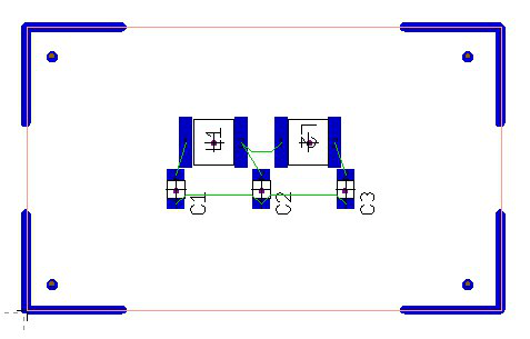
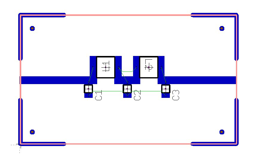
Step 7:
Now you first place the middle capacitor C2 in the center marked in this way. Please do not forget to activate the “Mount SMD on top” option when selecting the “1206” housing and then use the “d” key to turn the component 90 degrees before placing it down.
This is how the center of the microwave PCB board looks immediately before the capacitor is set down.
Step 8:
For both coils we choose the SMD housing 2220 and arrange them as shown in the picture opposite. However, please show the air lines beforehand (= level 27) and turn the components so that the air lines match the wiring correctly. And not the option “populate SMD on top …”
to forget.
Step 9:
Now it’s time to connect the two outer capacitors, which are placed below the coil connections.
Step 10:
Now we can delete our two “auxiliary lines” and pull three pieces of cable with a width of 1.83 mm as “microstrip wiring” from the left to the right edge.
First like this …
then like this!
Step 11:
Now we give each capacitor a nice field of 5 vias for its ground connection.
Do you remember? You have to move the cursor to the intended position and then press the “dot” on the keyboard twice in succession. Then the additional connecting wire is cut with “ESCAPE”.
(A bore diameter of 0.6 mm, an aura of 0.3 mm and a diameter of 1.5 mm were selected).
Step 12:
And because this is already working well, we lay out two small carpets in the upper half for earthing the coil shielding cups.
Step 13:
From the drawing tools (= button with the pencil) we get the “filled rectangle” and press “o” for the options. The rectangles must be on level 16 (= copper on top) and should combine all five vias of a ground connection.
Fortunately, the holes in the vias are automatically kept free by the program – we don’t have to do anything about that.
Step 14:
You should never forget that:
a suitable label on the upper copper side (level 16) must be, because otherwise the microwave PCB manufacturer does not know what is up or down and we may get A “mirrored” board may have been supplied.
We also find the text option behind the button with the pencil.
Step 15:
And to make things round, we go behind the “button with the magic wand” to activate the mass area filling option.
We release the lower side (level 2 = copper below) and select the signal “GND”.
Then the program is started.
That’s how it looks like.
Last step:
To print the top of the board, we only switch to levels 16 (= copper on top), 23 (= outline) and 24
(= Boreholes). Then we can take a closer look at what the microwave PCB board will look like.
Qualification and performance specifications of Microwave PCB
IPC-6012, qualification and performance specification for rigid printed circuit boards and IPC-6013, qualification and performance specification for flexible PCB.
Typically, the IPC tries to update these three qualification and performance specifications at the same time. IPC-6018 was published in January 2002 issue “A”.
Microwave PCB Material
The market for microwave technology has significantly fewer users than conventional PCB technologies. There are only a small number of PTFE suppliers, the Teflon material that is often used for micron wave substrates. The is in high contrast to the many enterprises, the wire plate on the basis of FR-4 laminates. However, when it comes to the use of materials, the term “small number” quickly becomes relative in the huge electronics industry. Numerous microwave PCB boards are now in use.
Microwave PCB Application
“This technology is used in many commercial applications such as cellular base stations and military products today,” said Michael Luke, chairman of the IPC D-22 subcommittee that developed the IPC-6018 directive.
As semiconductor chip speeds continue to increase, microwave technologies will also be required in other areas.
Microwave PCB Producing Guidlines
The additions deal with numerous changes regarding the circuit board substrate materials and the conductor tracks on them. The conductor tracks in the microwave range have significantly different performance parameters than those used for conventional circuit boards. Many traces of a typical microwave PCB board can be designed according to the IPC requirements for rigid and flexible circuit boards. In the areas in which high-speed microwave signals are present, however, completely different parameter values apply for conductor width, thickness and spacing. There is therefore no question that a different guideline must be used when procuring microwave printed circuit boards.
There are also differences in the substrates. In contrast to the FR-4 substrates of conventional printed circuit boards, most microwave PCBs are based on PTFE (Teflon). PTFE laminates have their own properties when individual layers are laminated. The dimensional stability is completely different, i. H. Designers and manufacturers need to take this into account when layouting circuit boards and positioning buried holes or blind holes or other elements that require drilling.
When these holes are drilled, resin residue known as “resin smear” may remain when the hole wall is formed. “The IPC-6018B guideline contains special criteria for the removal of resin residues (resin smear), which take into account the special properties of high-frequency circuit board laminates. It’s a big issue with PTFE circuit boards, ”said Perry.
Since the completion of Issue A in early 2002, numerous other changes have occurred. The developers of the directive have added reference information on passive resistors and capacitors to section 3 [REQUIREMENTS]. The new version has also improved the requirements for soldering edge breaks, which can arise whenever holes are not drilled in the middle of the pads. The subject of thermal stress has also been revised to take account of the progress made by convection reflow processes for thermal stress tests on ground specimens or samples from production printed circuit boards.