Modern electrical and electronic products and components are characterized by state-of-the-art technologies and offer users functions and services that were unthinkable only a few years ago. But despite state-of-the-art technology and manufacturing, errors and failures of electrical and electronic products and components occur again and again in practice, which brought us to today’s topic: PCB failure analysis!
The reasons for this are manifold and range from inadequate design to poor material quality to inaccurate manufacturing specifications. Unfortunately, however, errors and failures in electrical and electronic products are often not only an inconvenience but can be accompanied by considerable risk to people and the environment.
What is a PCB failure analysis
The term PCB failure analysis represents a comprehensive investigation of the causes that led to the failure of a product or component. Using a wide range of techniques and test methods, test engineers identify and evaluate the specific causes of the failure of a product or component.
Once the cause is determined, measures can be taken to modify or redevelop the product to avoid product failure in the future. Some error analysis methods can also be used in the prototype phase to detect potential errors early and address weaknesses before a product is launched.
Why are PCB failure analysis important
Product failures have a number of consequences for manufacturers of electrical and electronic products and components. Products that do not work as promised can lead to disappointed users and damage a company’s reputation as a manufacturer of high-quality products. However, product failures can also lead to costly and time-consuming product recalls and the associated negative publicity.
In the worst case, product failures endanger people and property and cause injury or even death. Fault analysis helps manufacturers improve the quality and safety of their products and reduce the risk of future failures on similar devices.
What can MOKO Technology do for your PCB
For Fault Analysis, we offer the full range of testing services for electrical and electronic products and components. In addition to fault analysis, we also offer the following testing services:
Coating tests/thin-film technology
– including determination of chemical composition, layer thickness, orientation and quality of the coating as well as adhesion tests.
Testing of printed circuit boards – e.g. determination of the thickness and homogeneity of the galvanizing layer, delamination tests and testing of solder heat resistance
Product testing
– e.g. radiation tests to determine the structural condition or to determine internal defects, electrical characterization by curve testing, dye-and-pry test in a ball grid array (BGA) and connections, and investigation of solderability.
Reliability and operational safety testing, including Investigations after temperature change and shock tests, moisture tests and salt mist tests.
Surface analysis
– x-ray photoelectron spectroscopy (XPS) and atomic force microscopy (AFM) and other methods
Thermal analysis using Differential Scanning Calorimetry (DSC), Thermogravimetric Analysis (TGA) and Thermomechanical Analysis (TMA) and other methods.
Chemical analysis
– including mass spectrometry with inductively coupled plasma (ICP-MS), Fourier transformation infrared spectroscopy (FTIR) and gas chromatography with mass spectrometry coupling (GC-MS).
Mechanical tests, including tensile tests, fatigue tests and vibration tests.
Electromagnetic compatibility tests (EMC)
– with regard to line and radiation emissions as well as immunity.
Cracks in the metallization of printed circuit boards
Problem: Electronic module failed
Solution: Metallographic cross-cutting
Result: Cracks in Via metalization
Flip-Chip Contacts
Example from Project HTM
Flip-chip contacts after oil test,
13346, NiAu/SbSn/PdAg,
2000 h at 200 °C
Deposits on printed circuit boards
Investigation of deposits
Methods: FTIR results:
Carboxylates (salts of carboxylic acids,
specifically adipic acid (hexanoic acid) and IC
Investigation of deposits
Method: REM and EDX
Bondabliftber
Fault analysis of multi-layer printed circuit boards
Problem: A sensor on a printed circuit board thermal stress no longer electrical contact
Solution: Metallographic cross-cutting
Result: A Wedge-Bond contact was lifted
Cause: Cracking between PCB and Gloptop resulted in mechanical stress.
Contamination
Description:
Contamination and corrosion on the copper surface caused problems with the tinning of this soldering eye. In addition, defects (bright areas) are visible on the copper surface, on which base material shines through (layer thickness of the copper is too thin). Unacceptable error, as non-soldering may occur in the later soldering process.
Causes/remedial work:
• Manufacturer’s manufacturing electrical defect
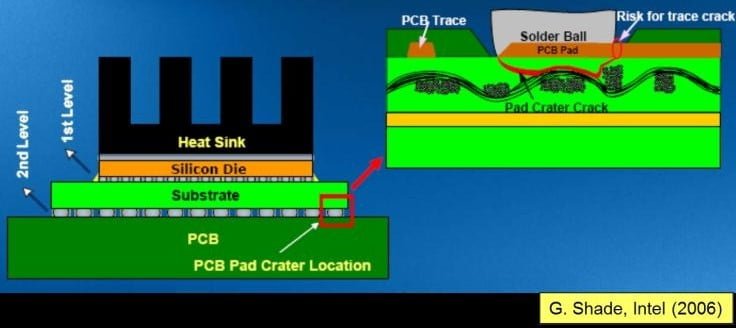
The crater on a component
Gold layer
Description:
Errors in the electroplating process. At the marked areas, too little gold was deposited galvanically. The underlying layer (Ni) shows the first signs of corrosion. Intolerable error, as soldering errors, can occur in the soldering process.
Causes/remedial work:
• Electroplating process deficient
• Preparation of the printed circuit board (cleaning, underlayers) deficient
Defective gold layer
Knot formation
Description:
Knot formation of the Ni-Barrier layer under the gold surface. Due to unfavorable current distribution in the electroplating process, many nodules formed in the middle layer (see lower picture, cut) that protrude through the gold layer. In the overview, these nodules are clearly visible. This circuit board should not be used as soldering or contact problems are to be expected.
Causes/remedial work:
Electroplating process deficient medium Ni layer breaks through the upper gold layer
Knot formation
Interruption
Description:
Interruption of a trace. Due to errors in the galvanic process during the production of the printed circuit board (subtractive process), part of the trace was etched away. This error is an indication of flaws in the photoresist. Manufacturing error.
Electroplating errors in the production of the PCB
Error in the manufacturer’s photoresist/process error
Partial interruption
Description:
Same connection as shown above, however, the trace is not completely separated. Although the electrical function is given, problems with the function of the printed circuit board may occur later under electrical load conditions.
Electroplating defects in PCB production
Error in the manufacturer’s photoresist/process error
Partial interruption of a conductor’s track
Foreign particle inclusion
Description:
Inclusion of a foreign particle in traces. This is probably fiberglass of the base material. Because this inclusion reduces the trace thickness, this error is not acceptable.
Causes/remedial work:
Failure to manufacture PCB
Uneven paint surface
Causes/remedial work:
• Cover mask unsuitable
• Contamination of surfaces on the printed circuit board
• Heat load on the paint deficient
Causes/remedial work:
• Errors in the coating process of the paint
• Stripping of the varnish deficient
Description:
The offset of the coating compared to its ideal position. This most common error has a very large influence on the later solder quality, because (as shown in the picture) the wettable surfaces can be significantly reduced or completely obscured. Intolerable error.
The offset of the cover coating
Description:
The offset of the coating compared to its ideal position.
Causes/remedial work:
Errors in the coating process of the paint
Stripping of the varnish deficient
Error layout-related (exposure)
Inclusion
Description:
Inclusion of undefined particles under the paint. Short circuits (electrically conductive inclusions) will be caused by this error.
Causes/remedial work:
Manufacturer’s manufacturing error
Contamination of the uncoated base material
Defects
Description:
Partial flaws in the coating, the irregular layer thickness of the coating. This error can only be observed in casting processes. Due to the uneven distribution of the paint on the printed circuit board, there were also defects (complete absence of the paint). Uncovered conductor pulls may cause corrosion that can affect the electrical behavior of the assembly.
Causes/remedial work:
Paint process deficient
The used cover varnish is not suitable
The surface of the base material not flat, the poor spread of the paint
Defects in the coating
Description:
Malfunction of the paint directly on a trace. In the soldering process, there is a risk of building bridges between the soldering eye and the wettable trace surface. This phenomenon is mostly due to the impurities of the underlying printed circuit board areas. Rework is required.
Causes/remedial work:
Impurities (fats) of the PCB
Errors in the painting process that lead to partial defects
mechanical effects on the paint (flasion of the paint)
Cracks
Description:
Cracks (microcracks) on the surface of the solder stop mask. Errors in the processing of the cover mask (stresses, bulging of the base material) create cracks in the paint surface. The main problem is the subsequent penetration of moisture due to corrosion on the ladder surfaces. Corrosion is particularly problematic for current-flowing conductors because electrical migrations strongly negatively affect the insulation resistance.
Causes/remedial work:
Solder stop cover deficient
mechanical loads lead to cracks in the paint
Failed to process the paint
Cracks in the paint
Description:
The same connection as above, however, the cracks were mechanically induced here, e.g. by transport influences.
Causes/remedial work:
Improper handling of the printed circuit board/assembly
Cover lacquer not resistant to mechanical loads
Detachments, wrinkles
Description:
Detachments, wrinkles around two solder-filled through-contacts. The thermal load in the soldering process, coupled with a poor layout design (the paint is too close to the through-contact), led to the shown removals of the paint.