PCB layout design is a key step in the manufacture of circuit boards. A reasonable PCB layout is conducive to controlling the production cost and ensuring high reliability. On the contrary, an unreasonable PCB layout can not meet the manufacturability, making the PCB function limited or even causing a variety of problems, such as circuit failures, which increase the manufacturing cost and delay the production time. Nowadays, people have higher and higher requirements for electronic devices, and PCBs used are more and more complex and compact. A small PCB needs to achieve multiple functions, which undoubtedly brings greater challenges to PCB layout design. And there are a number of aspects to consider in PCB layout design. In this article, we have explained the PCB layout design process, listed the most critical aspects that should be considered during the design, as well as some common problems to be avoided. Let us read on.
What Are the Steps for PCB Layout Design?
Creating a functional printed circuit board (PCB) requires careful planning and execution across many phases. It’s a collaborative effort between electrical engineers, mechanical engineers, PCB designers, and manufacturers. Here is a more in-depth look at the end-to-end PCB design process:
- Develop the schematic diagram.
The schematic captures the electronic circuit conceptually, mapping out PCB components like resistors, capacitors, integrated circuits and their interconnections without regard for physical layout. Schematic capture software is used to digitize the schematic for PCB design.
- Select the board stackup.
This refers to the layering and composition of the PCB itself. Factors like number of layers, dielectric materials, copper thickness and trace width impact parameters such as impedance, which affects signal integrity. The stackup must be compatible with circuit performance needs.
- Outline design rules and manufacturing requirements.
PCB fabrication has strict standards set by organizations such as IPC. These cover minimum trace spacing, hole size, mask overlay and more. Having a PCB partner well-versed in these specifications helps avoid errors or faulty boards.
- Arrange components and footprints.
With the schematic as a guide, PCB layout begins by placing component footprints and assigning reference designators. Placement guidelines help minimize electrical noise and interference. Component data sheets provide details needed for positioning and orientation.
- Include drill holes for vias and pins.
Vias provide vertical interconnects between layers. Many double-sided flex circuits require plated through holes. Hole dimensions and locations are specified.
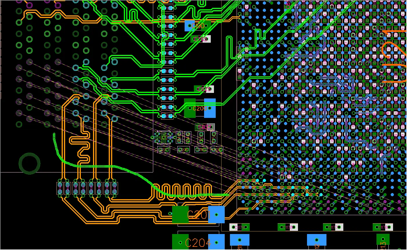
- Connect traces for conductors.
Traces are the copper lines that form the conductive pathways between different components according to the schematic layout. Auto-routing tools assist with this but often manual routing is required.
- Integrate testpoints, labels and markings.
Testpoints facilitate testing and troubleshooting. Identifiers, polarity markings, version numbers and other text information are added, usually by silkscreening or engraving.
- Verify design rules and generate manufacturing files.
The completed board layout undergoes final checks for any violations of design rules. Then fabrication and assembly files are output, containing all necessary PCB manufacturing data.
With the design fully defined, the PCB moves forward to the fabrication stage, where the electronic blueprint gets transformed into a physical board ready for population with components. The entire process requires close collaboration between many disciplines.
Key Considerations on PCB Layout Design
The Size&Shape of Bare Board
The first thing to consider in PCB layout design is the size, shape, and number of layers of the bare board. The size of the bare board is often determined by the size of the final electronic product, and the size of the area determines whether all the required electronic components can be placed. If there is not enough space, you may consider using a multi-layer or HDI design. Hence, it is crucial to estimate the board size before starting the design. The second is the shape of the PCB. In most cases, they are rectangular, but there are also some products that require the use of irregular-shaped PCBs, which also have a great impact on the placement of components. The last is the number of layers of the PCB. On the one hand, a multi-layer PCB can allow us to carry out more complex designs and bring richer functions, but adding one more layer will increase the production cost, so it must be determined early in the design. specific layers.
Manufacturing Processes
The manufacturing process for producing the PCB is another important consideration. Different manufacturing methods bring different design constraints, including the PCB assembly method, which must also be considered. Different assembly technologies such as SMT and THT will require you to design the PCB in different ways. The most critical thing is to confirm with the manufacturer that they are capable of producing the PCB you need and that they have the skills and expertise needed to implement your design.
Materials and Components
In the process of design, it is necessary to consider the materials used and whether the components are still circulating in the market. Some parts are difficult to find that are time-consuming and expensive. It is recommended to use some more common components for replacement. Therefore, the PCB designer must be experienced and knowledgeable about the entire PCB assembly industry. MOKO has a professional PCB design and component procurement team. Our professional knowledge and complete procurement chain allow us to select the most suitable materials and components for customers’ projects, and provide the most reliable PCB design within the customer’s budget. In addition, you can check out our other blog to know more information about PCB materials: https://www.mokotechnology.com/pcb-material/
Component Placement
PCB design must consider the order of component placement. Properly organizing component positions can reduce the required assembly steps, improve efficiency and reduce costs. Our recommended placement order is connectors, power circuits, precision circuits, critical circuits, and lastly the rest of the components. In addition, we should also notice that excessive heat dissipation from the PCB can degrade performance. When designing the PCB layout, consider which components will dissipate the most heat, keep critical components away from high-heat components, and then consider adding heat sinks and cooling fans to lower the component temperature. If there are multiple components that generate heat, these components need to be distributed in different locations, and they cannot be concentrated in one location. On the other hand, the direction of placing the components also needs to be considered. Generally, similar components are recommended to be placed in the same direction, which is conducive to improving the efficiency of welding and reducing errors. It should be noted that the parts should not be placed on the solder side of the PCB, but should be placed behind the plated through-hole parts.
Power and Ground Planes
Power and ground planes should always be kept inside the board and should be centered and symmetrical, which is a basic guideline for PCB layout design. Because this design can prevent the circuit board from bending that makes components shift from their original position. Reasonable placement of power ground and control ground can reduce the interference of high voltage in the circuit. We need to separate the ground planes of each power stage as much as possible, and if unavoidable, at least ensure that they are located at the end of the supply path.
Signal Integrity and RF Issues
The quality of PCB layout design also determines the signal integrity of the circuit board and whether it will be subject to electromagnetic interference and other issues. To avoid signal problems, design to avoid running tracks parallel to each other, as parallel traces will have more crosstalk and cause various problems. And if the tracks need to cross each other, they should be crossed at right angles, which reduces the capacitance and mutual inductance between the lines. Also, if components with higher electromagnetic generation are not required, it is recommended to use semiconductor components that produce low electromagnetic radiation, which also helps with signal integrity.
Common Mistakes to Avoid in PCB Layout Design
Ignoring cooperation with manufacturers
It’s a common misunderstanding that many engineers think it’s fine to just give the design files to the manufacturer before starting manufacturing. In fact, it is better to share it with the manufacturer when the first draft of the PCB layout is designed. They will review the PCB design according to their rich manufacturing experience and find problems that you can’t find, so as to ensure the manufacturability of the design.
Too close to the edge
The components cannot be too close to the edge of the circuit board, and they need to be kept at a suitable distance, otherwise, the components are prone to break due to being too close to the edge. And this problem, experienced manufacturers can often find when they get the design files and ask engineers to make changes, such as placing a route around the edge to solve the hidden danger.
Ignore the verification of the PCB layout design
When it takes you a lot of time and energy to complete the PCB design, you just cannot wait to enter the production process, then you are wrong. The verification of the PCB design must not be ignored, otherwise, it will bring big trouble. Imagine waiting until PCB production has already started to find the problem, it will waste a lot of time and bring greater economic losses. Therefore, we need to verify the design multiple times to ensure that there are no errors before it can be put into production. We suggest performing Electrical Rules Checking (ERC) and Design Rule Checking, these two systems can help us verify if designs meet common manufacturing requirements, high-speed electrical requirements, and more, and identify potential design problems early and correct them quickly.
Complicates PCB Design
Some complex designs should be avoided as far as possible unless it is essential, otherwise, it will take extra time and cost to manufacture. For example, undersized parts will complicate production. If the board has enough space to accommodate larger components, large-sized components should be selected, which is more in line with product manufacturability. In short, it is much better to spend more time in the design stage to make the layout simpler and meet the functional requirements, which will be beneficial to improve production speed and quality.
Team Up With A Turnkey PCB Supplier
All in all, PCB layout design is not an easy job, if you are not proficient in it, then maybe you can ask for help from a turnkey PCB supplier. Besides manufacturing, they also specialize in PCB design and engineering.
MOKO Technology provides one-stop PCB solutions, from PCB design to production, assembly, and testing, we have got you covered. We have a professional engineering team with more than ten years of experience in the PCB industry, designing and producing PCBs for customers from various industries. If you are not sure if your PCB design is sound, please contact us, and our experts will evaluate your design and make manufacturable suggestions. Or you can outsource the PCB design service to us and we can turn your idea into a product in the shortest possible time.