Advancements in technology continue to push the boundaries of PCB design, demanding smaller and more complex layouts. When it comes to creating intricate connections within a circuit board, two techniques have emerged as key players: blind via and buried via. These innovative via technologies have revolutionized the way electrical signals flow through circuit boards, allowing for greater density and improved performance. In this blog, we will explore the features and applications of blind vias and buried vias, compare the differences between them and provide insights about how to choose the right via for your PCB layout.
What Is Blind Via?
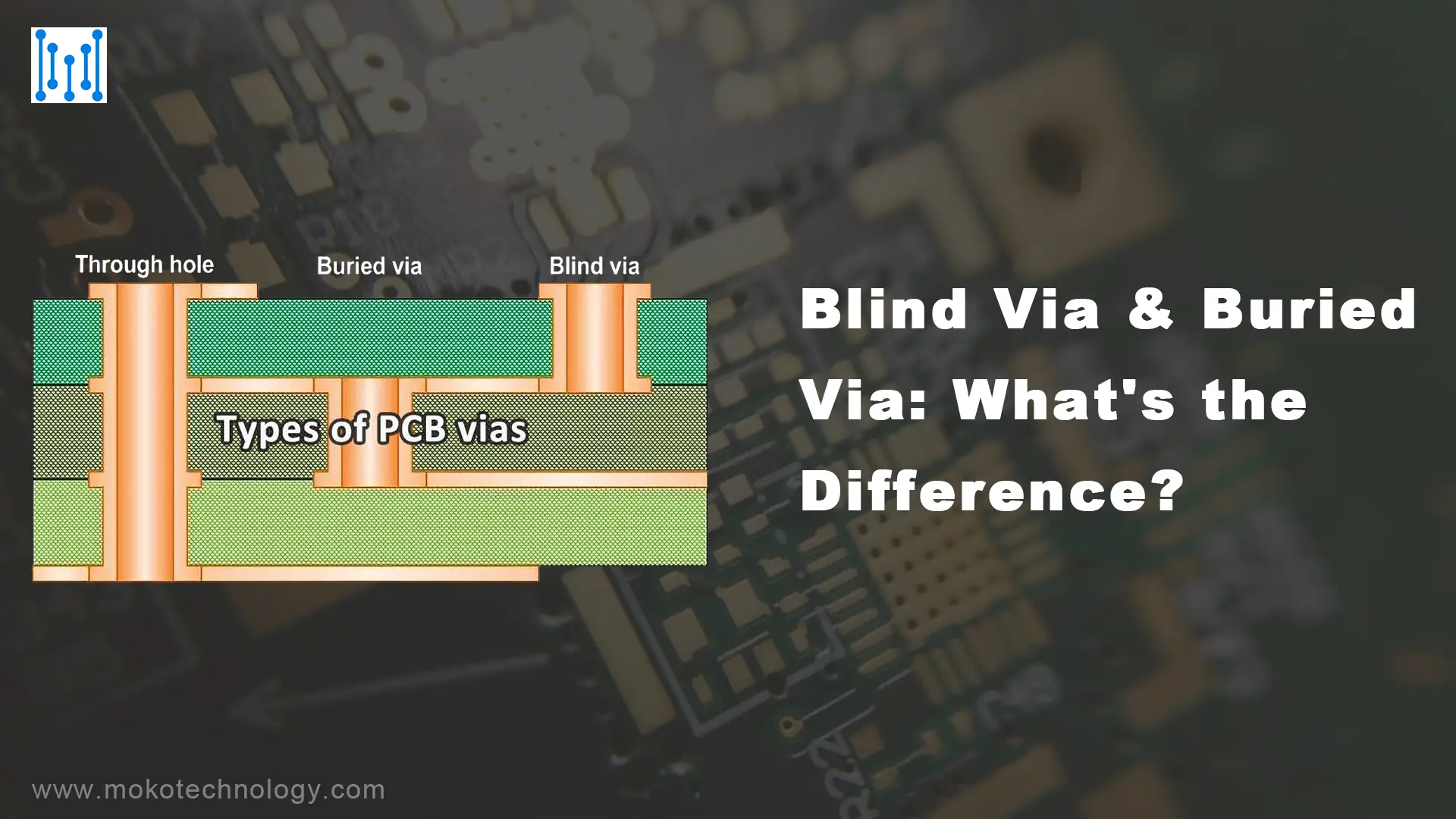
A blind via is a type of drilled hole used in printed circuit boards (PCBs) that connects the outer layers of the board to one or more adjacent inner layers. Unlike a through-hole via that traverses the entire board, a blind via only extends partway into the PCB and does not emerge on the opposite side. It allows for the routing of signals or power connections between specific layers while conserving valuable board space. Blind vias are typically manufactured using specialized drilling and plating techniques to achieve the desired depth and connection.
Applications of Blind Vias
Blind vias find extensive applications in various industries where space constraints and high-density circuit designs are crucial. Here are some notable applications:
Mobile Devices: With the ever-increasing demand for smaller and more compact mobile devices, blind vias enable the efficient interconnection of complex multilayer PCBs found in smartphones, tablets, and wearable gadgets.
High-Speed Communication: Blind vias play a crucial role in high-speed communication systems, such as routers, switches, and network equipment. They facilitate the transmission of signals between different layers of the PCB, reducing signal distortion and improving overall signal integrity.
Consumer Electronics: From gaming consoles to digital cameras, consumer electronics often rely on blind vias to achieve miniaturization without sacrificing performance. These vias enable designers to create intricate and densely packed circuitry, enhancing functionality and reducing the size of the final product.
What Is Buried Via?
Buried vias are drilled holes that connect only the inner layers of a multilayer PCB without extending through to the outer layers. They are entirely encapsulated within the PCB and cannot be accessed from either side of the board. Buried vias are used for interconnecting inner layers, enabling complex multilayer interconnections while maintaining signal integrity and minimizing signal loss. They are especially useful in designs where maintaining a continuous outer layer surface is crucial, such as in high-speed and high-frequency applications.
Applications of Blind Vias
Buried vias offer unique advantages in specific applications that require enhanced reliability and signal performance:
High-Density Interconnects: Buried vias are commonly employed in high-density interconnects, where multiple layers of circuitry need to be interconnected while maintaining signal integrity. They are often used in advanced PCBs for aerospace and defense applications, medical devices, and high-performance computing.
RF/Microwave Applications: Buried vias play a critical role in RF/microwave circuitry, where signal loss and interference must be minimized. These vias provide a controlled and stable impedance path for high-frequency signals, improving the overall performance of wireless communication systems, radar systems, and satellite communications.
High-Reliability Applications: Industries such as automotive, aerospace, and industrial automation demand robust and reliable circuit boards. Buried vias offer improved mechanical strength and resistance to environmental factors like temperature and humidity, making them suitable for applications where durability and longevity are essential.
Advantages and Disadvantages of Using Blind Via and Buried Via
Advantages
- Increased density
Blind vias allow for connections between outer and inner layers, conserving valuable board space. They enable designers to achieve higher circuit density and more compact PCB layouts.
- Reduced Manufacturing Cost
Blind vias can help reduce the cost of PCB manufacturing by minimizing the number of layers needed for routing. This reduction in layer count can lead to cost savings in terms of material, manufacturing processes, and overall production time
- Improved signal performance
By reducing the length of the via, blind vias help minimize signal distortion and improve signal integrity. They can be strategically placed to optimize signal paths and minimize interference.
Disadvantages
- Manufacturing difficulty
The use of blind vias requires precise drilling and plating operations, which can result in increased manufacturing costs and complexity for the PCB. Achieving the desired depth and accuracy in blind via drilling and plating processes demands specialized equipment and expertise, which may incur additional expenses.
- Layer count restrictions
Blind vias can impose restrictions on the number of layers that can be utilized in a PCB design. Since blind vias only connect the outer layers to specific inner layers, they limit the number of layers available for routing and interconnection.
The Differences between Blind Via and Buried Via
- Purpose and Function
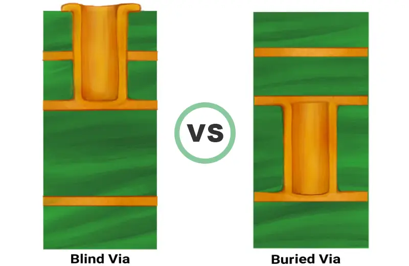
Blind Via: Blind vias are primarily used to connect the outer layers of a PCB to one or more adjacent inner layers. They allow signals to pass through different layers while conserving valuable board space. Blind vias help achieve higher-density circuit designs in PCBs.
Buried Via: Buried vias are used solely for interconnecting inner layers of a multilayer PCB. They do not connect to the outer layers. Buried vias are effective in achieving complex multilayer interconnections while maintaining signal integrity and minimizing signal loss.
- Manufacturing Complexity
Blind Via: Manufacturing blind vias involves drilling from the outer layer and stopping at a specific inner layer. It requires special drilling and plating techniques, including controlled depth drilling and plating processes, to create the desired blind via structure. This complexity can impact manufacturing time and cost.
Buried Via: Manufacturing buried vias involves drilling between inner layers, typically after all inner layers have been laminated together. This drilling is followed by a plating process to create the via structure. Buried vias can be more complex to manufacture compared to blind vias due to the need for precise drilling and plating within the multilayer stack-up.
- Design Flexibility
Blind Via: Blind vias offer more design flexibility as they connect the outer layers to specific inner layers. Designers have greater control over the placement and routing of blind vias to optimize signal paths and minimize interference.
Buried Via: Buried vias provide less design flexibility as they are confined to interconnecting inner layers only. Their placement and routing are determined by the specific layer stack-up of the PCB.
- Cost Considerations
Blind Via: Blind vias can be more expensive compared to traditional through-hole vias due to the additional manufacturing steps involved in their creation. The complexity of drilling and plating processes for blind vias can contribute to higher fabrication costs.
Buried Via: Buried vias can also add to the manufacturing cost of a PCB, especially in cases where complex multilayer stack-ups are required. The drilling and plating processes for buried vias can raise the total manufacturing cost. Generally, buried vias tend to have higher manufacturing costs compared to blind vias. The manufacturing process for buried vias is more complex and involves additional steps compared to blind vias.
Choose the Suitable Via for Your PCB Layout
Careful consideration of various factors is necessary when choosing between blind vias and buried vias for your PCB design. To determine the best via option, you should evaluate the specific requirements of your design, such as space constraints, signal integrity needs, and manufacturing capabilities. If space is limited and you require high-density routing, blind vias are a suitable choice as they connect the outer and inner layers while conserving board space. On the other hand, if signal integrity is critical, especially for high-frequency or sensitive signals, buried vias provide better performance as they are fully encapsulated within the PCB. Additionally, it’s essential to assess your PCB manufacturer’s capabilities and limitations, including their ability to handle blind vias or buried vias, minimum hole sizes, and aspect ratios. MOKO Technology, a leading PCB manufacturer, offers extensive expertise in PCB vias. With our advanced capabilities and experience, we provide reliable solutions for PCB vias, ensuring optimal performance and quality in your PCB designs.