PCB Milling boards
Boards (circuits boards, printed circuit boards, …) can be manufactured in many ways, in this article, there’re two PCB milling ways we would like to introduce. The first way goes like this:
• Making a movie
• Exposure of the photosensitive base material
• Develop
• Etching
• Drilling
• Decoating
• Coating with soldering varnish
PCB Insulation milling
The second way of PCB manufacturing-PCB milling , which at first seems more attractive, is insulation milling. This requires the following steps:
• Generating the milling data, preferably as G-code according to DIN 66025
• Clamping the base material
• Milling the contours of the conductor tracks
• Drilling the holes for the components in the same clamping
• Coating with soldering varnish
The following points speak for the insulation milling:
• The basic PCB material is cheaper
• The panic with chemicals falls away
• The production of a single PCB prototype is faster
On the other hand, it speaks against:
• You need an appallingly expensive CNC milling machine, along with the necessary control electronics and PCB software. Nothing should go below 2,000,- Euro total costs, even in self-construction. As a PCB manufacturer in China since 2006, MOKO Technology manufactures PCB with advanced CNC milling machines to assure good quality
• Expensive carbide cutters are required for milling, which usually last only 1 – 2 European boards
• Creating the milling data is not easy
• Setting the PCB milling parameters is difficult and usually only works with trial and error
• Milling a one-sided European board can take more than an hour
• The milling dust (glass fibres!) may be harmful to health
PCB manufacturing procedure
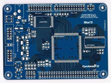
If you still want to mill your printed circuit boards, here is the procedure you can use to produce the board shown above with the dimensions 100 mm x 60 mm. This is the control board of the spindle motor of milling machine. The board is only one-sided, but the production of double-sided boards is possible according to the same process. It is important that a trace width can be created, which makes it possible to perform a trace between two IC connections. Otherwise, only very simple boards can be milled. The fact that it can be succeessful in this shows the following cut-out enlargement:
The trace width should be around 0.3 mm, the distance between the traces and soldering eyes about 0.4 mm. This means that the PCB board can also be soldered sensibly without constantly soldering traces with each other. However, this requires a decent soldering iron with a thin, long tip and good soldering wire (0.5 mm).
The software pcb-gcode
Without appropriate software, of course, nothing works. You can use the layout software Eagle to design the printed circuit boards, of course, if you find MOKO Technology, you can get PCB design as free with your PCB manufacturing need. Eagle has a freeware version for trying out and for smaller projects. This is also interesting for people who use a different layout program, as we will see later.
However, creating PCB milling programs for insulation milling is not a standard function of Eagle. But because it is possible to have such functions carried out by so-called “ULPs” (User Language Programs), a man named John Johnson has earned himself to write a suitable ULP.
The ULP can be downloaded from the CadSoft download page. First, look for the “pcb-gcode.zip” ULP. Unfortunately, there is no search function, but the ULPs are sorted alphabetically. Download the zip file and unzip all the files it contains to the c:-programs-EAGLE-4.12-ulp directory.
Now, if you type “run pcb-gcode -setup” in Eagle’s layout view on the command line, the following configuration screen should appear:
Here you set the following parameters:
1.Top Side (top of the PCB board, side of the component)
• Generate top outlines – Generate PCB milling data for the conductor tracks of the top
• Generate top drills – Create drilling data for the top
• Generate top fills – Create milling data to remove all copper between traces and soldering eyes (usually not required)
2.PCB Bottom Side (bottom of the board)
• How the parameters of the top
3.PCB Board (parameters that apply to the entire board)
• Generate Milling – generates milling data from the mill layer of the board (e.g. outline or larger cutouts)
• Isolation Default – this should be a very small value, 0.0025 is OK
• Isolation Maximum – the maximum width of the insulation
• Isolation Step Size – how much wider the insulation becomes with each pass
4.CB Units (units of measure)
• Microns – thousandths of a millimeter
• Millimeters – millimeters
• Mils – Thousandths of An inch
• Inches – inches (25.4 mm)
Then click on the “Machine” tab. The following window appears:
Here you set the following parameters:
5.Z-Axis (Z-Axis settings)
• Z High – A position that avoids collisions with clamping devices
• Z Up — The position on which the Z axis is driven over the board when positioning in a hurry. Should not be chosen too high to save time
• Z Down – Intrusion depth of the cutter
• Drill Depth, slightly more than the thickness of the printed circuit board
• Drill Dwell – Bore time
• Milling Depth – PCB Milling depth for outlines and cut-outs, slightly more than the thickness of the board
6.Tool Change
• Position on which the Z axis is driven for convenient tool change
Spindle (milling spindle)
• Spin Up Time – Time in seconds to keep the spindle at speed
• Etching Tool Size – Width of the engraving stitch for milling the trace outlines (see below)
7.Feed Rates
• XY – Feed speed for the X and Y axes during PCB milling
• Z – Immersion speed of the cutter
Then click on the “GCode Style” tab. The following window appears:
Here you can now set for which PC control program the code should be generated. This is what a so-called “post processor” (.pp) does. As a fan of Mach3, I chose “Mach”. If there is no post processor for the control program you are using, you can create one yourself by doing the following:
• Choose the post processor that comes closest to the desired one
• Then open the gcode-defaults.h file in the directory C:-Programs-EAGLE-4.12-ulp with the editor
• Mmake the necessary changes
• Do not change the format codes such as “%f”, “%d”, etc.
• Save the file under a new name, e.g. “Cover.pp”
Then, when you click Accept, the configuration changes are saved. Clicking “Accept and make my board” saves the configuration changes and starts generating the milling and drilling data. Clicking “Cancel” discards all changes.
Generating PCB milling and drilling data in Eagle
Generating the data from Eagle is very easy, but some detail needs to be considered to create a usable circuit board. First, you should set the “Design Rules”. To do this, enter “drc” on the command line or click on the corresponding icon. The design rules window appears.
First, click on the “Clearance” tab and set all distances to 16mil (0.4 mm). This is first of all a good starting point for your own experiments. Then click on the “Sizes” tab.
Set the minimum track width to 16mil (0.4 mm). This is important when working with the Autorouter. Then click on “Restring”.
Set the pads (component connectors) to 16mil. This ensures that they do not become too small.
All values are those with which I work and with which I have achieved good results. Of course, you may be able to achieve better results with other values.
Then click “Check”. You will probably get a list of errors that complains of too few distances between the traces. Change the spacing accordingly. However, you can ignore too few distances where traces are performed between IC ports. They should not make the traces narrower there either.
If everything is fine, type “run pcb-gcode” on the command line
The following files are then generated, all of which have the name of your schematic file, to which the following extensions are attached:
• top.nc: the trace outlines for the top of the board
• bot.nc: the trace outlines for the bottom of the board
• tf.nc: Milling data to remove the remaining copper on the top (usually not necessary)
• bf.nc: Milling data to remove the remaining copper on the bottom (usually not necessary)
• td.nc: Drilling data, seen from the top. At the beginning there is a table with the required drill diameters. Due to the conversion inch millimeters with partly “crunch” values. Just take the drill that comes closest.
These are to be used in the production of one-sided boards, otherwise the board would have to be turned over.
mt.nc: Milling data for outlines and cutouts, seen from the top.
mb.nc: Milling data for outlines and cutouts, seen from the bottom.
These files are written to the same directory as your schematic file.
For a first test, you can now open the top.nc or bot.nc in Mach3 and view the result. Presumably, the display of the milling webs is outside the preview window. Therefore, reduce the size of the display until you see the board. Then move and move them until you have a clear picture:
Click on the image to see it in full size and check the outlines of the traces and component connectors. Particularly critical are the places where traces are carried out between component connections. If there is no milling track between the conductor track and the connection, then you must reduce the width of the milling stitch in the configuration (Etching Tool Size).
Clamping the board
To be able to mill the board, you must first clamp it. It makes a significant difference whether you work with an engraving depth controller or not. The engraving depth controller ensures that the PCB milling stitch always has the same immersion depth at all points of the board. Because the Stichel is V-shaped, the depth determines the width of the insulation, i.e. the milled web. If this becomes too wide, then your traces disappear into the nirvana, it becomes too narrow, copper stops and leads to short circuits. The depth controller on my machine looks like this:
The short pipe at the front is the connection for the vacuum cleaner, the micrometer screw is used for height adjustment. I will describe how the depth controller works and is built elsewhere.
Because the engraving depth controller presses the board firmly onthe underlay, it does not need to be secured against lift-off. Instead, it is important to secure the board against slipping. For this purpose, I have built a frame consisting of 1.0 mm rigid aluminium sheets on a wooden plate.
Two sheet metal strips form an angle into which the board is pressed by two wedges of the same material. The image should make the principle understandable. This type of fastening has the advantage for series production that the boards are always clamped in the same position. So I can first mill all the boards and drill them in one pass without having to constantly change the program and the tool.
The PCB milling tool
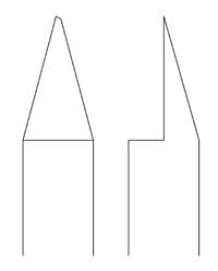
You can use engraving stitches for milling, which are parts made of carbide round rods, in which half is ground away in the lower area. These are then sanded at different tip angles. The grinding angle is always half the size of the tip angle. The tip is slightly sanded, resulting in a cutting edge. Cutting width and tip angle can be selected when ordering. So far, I have achieved the best results with 0.1 mm cutting width, a tip angle of 40° and a milling depth of 0.2 mm. The drawing shows a trick:
The shaft diameter should be 3 mm, which also fits with Proxxon collets. There are also stitches with 1/8 inch shaft diameter, which do not fit properly into the 3.2 mm collet and tend to “egg”. Take a look at eBay, there are several vendors. Make sure that you get stitches with a finished cut edge, you have to grind stitches without cutting with a stitch grinding machine yourself.
Workpiece zero point
The workpiece zero point is located on the left front edge of the PCB board in the milling data for the top. At the bottom, however, it is located on the right, front edge. All coordinate values of the X axis are negative!
Height
If you work with an engraving depth slider, you know how to adjust the height. Otherwise, the easiest way is to clamp a cutter and drive it over the board for a short time. Then loosen the chuck and drop the cutter onto the board. Then tighten the feed again and set the Z-axis to zero. Don’t forget to drive the Z-axis up a bit again!
Immersion depth
The immersion depth is very critical, because this results in the width of the PCB milling web. The formula for this is:
Cutter 40°: Width = Immersion Depth * 0.7279
Cutter 60°: Width = Immersion Depth * 1,1547
You need a certain minimum immersion depth (0.15 – 0.2 mm in my experience), otherwise a ridge will be created at the milled webs. Since inaccuracies of the machine also play a role, I advise to try some of the pieces of waste.
Spindle speed
The speed of the milling spindle should be as high as possible in order to achieve a burr-free cut. Spindle speeds from 20,000 rpm are OK. However, on my machine with 6,000 rpm also quite clean boards are available.
Milling
Now it’s time to start! Also pay attention to the necessary safety distance of the cutter and that there are no clamping means in the way. Don’t forget to turn on the spindle! You probably won’t be satisfied with the first result and will have to experiment a bit.
Drilling
One of the charms of the process is that you can drill the board immediately. To do this, you need the drilling data of the respective page. The holes go through the whole board in any case, but are mirror-image at the bottom to the top, i.e. also with the drilling data the zero point of the bottom is right front. As soon as a drill change is required, the PCB milling program stops and moves the spindle to the position you specified for the tool change.
Double sided PCB
As already mentioned, the production of double-sided boards is also possible. To do this, place a separate, small hole in the lauyout of the board and note the coordinates. To do this, enter “info” on the command line and click on the hole. You will then see a small window
The first coordinate (52.07) is the X axis, the second is the Y axis, seen from the top. If you turned the board after milling and drilling the top, position the center of the milling spindle exactly over this hole and enter the coordinate values as the X and Y positions in the controller. You have to enter the X-coordinate as a negative value!
Other PCB layout programs
If you are working with a different layout program, you can read the Gerber and Exellon data using the Eagle Power Tools and then generate the milling data from it, and as per a PCB manufacturer that you can trust, MOKO Technology can be a good choice as we’re professional in manufacturing and assembling printed circuit boards since 2006, we’re also open to answer any of your questions on the issues of your PCB boards!