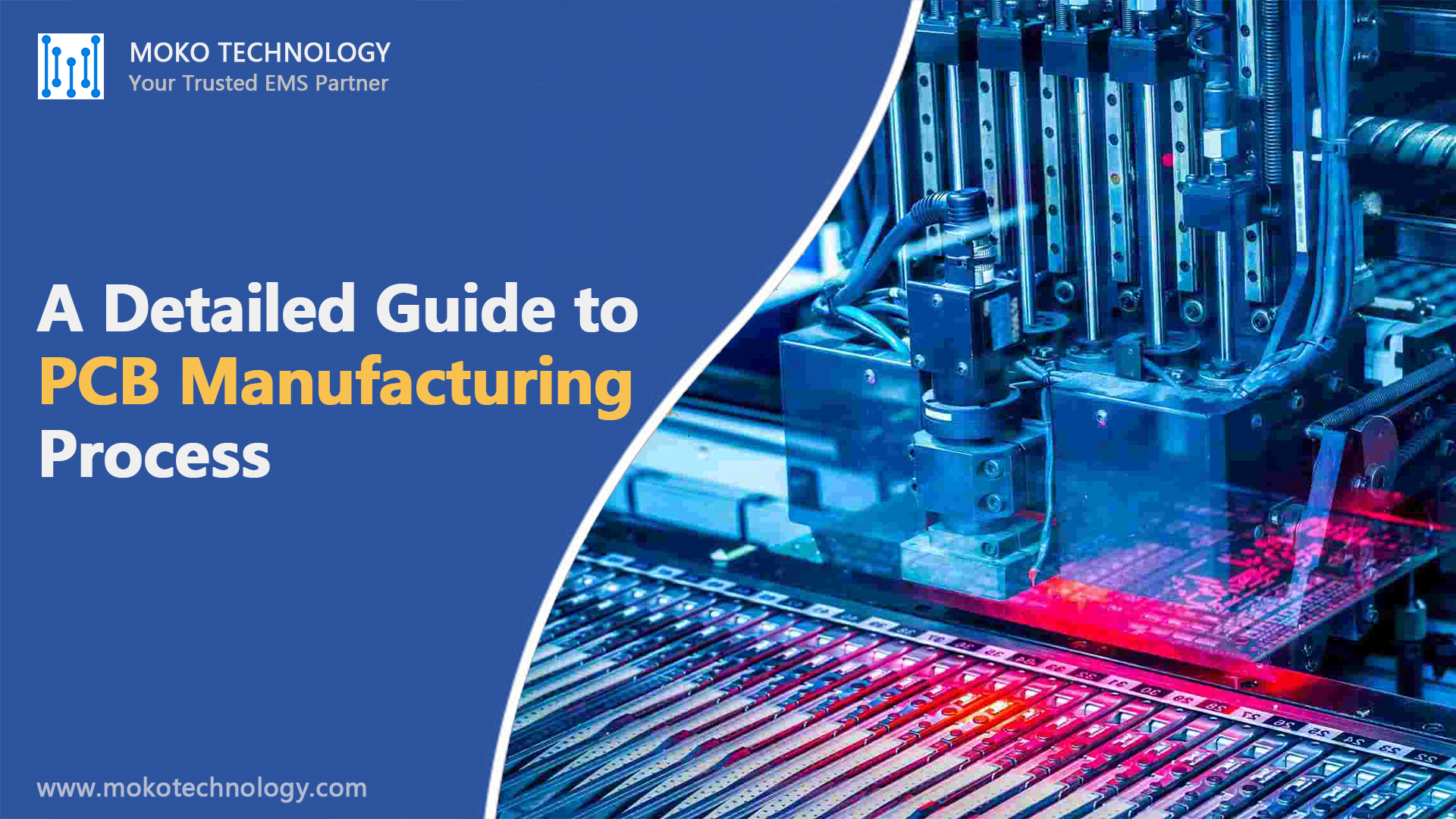
Introduction
PCBs (printed circuit boards) form the foundation of contemporary electronic devices, ranging from handheld devices like mobile phones to advanced spacecraft technologies. They are essential for connecting electronic components and providing a stable platform for them to operate on. PCB manufacturing is a complex process with several intricate steps, and each step is crucial and requires meticulous attention to detail to ensure defect-free printed circuit boards. The process commences by going through the design and review phases, using computer-aided design (CAD) tools for PCB circuit board design, and proceeds until the board is manufactured. To enhance efficiency and reduce the risk of human error, computer-guided and machine-driven techniques are implemented to avoid incomplete or short circuits. To guarantee high quality, the boards undergo strict testing at various stages of fabrication, including final testing as complete boards, before being packaged and shipped for delivery.
PCB Manufacturing Process-Step by Step
Step1: Design PCB
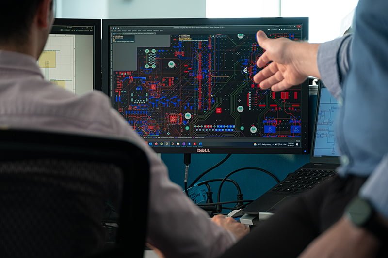
The first step for any PCB manufacture is to make the design. PCB manufacture and design always start with some sort of plan. The designer lays out a blueprint for the PCB that fulfills all the requirements as needed. Once a design blueprint for the PCB is encoded by the software, all the different aspects and parts of the design are checked again to make sure there are no errors.
Once the inspection by the designer is complete, the finished PCB design is sent off to a PCB fabrication house so that the PCB can be built. Upon arrival, the PCB design plan is undertaken with a second check by the fabricator, known as the Design for Manufacture (DFM) check. A proper DFM check confirms that the PCB design fulfills, at least, the tolerances required for manufacture.
Step 2: Print PCB Design
After all the checks are successfully completed, the PCB design can be printed. Dissimilar to other plans, like architectural drawings, PCB plans don’t print out on a regular 8.5 x 11 sheet of paper. Instead, a special printer, known as a plotter printer, is used. A plotter printer develops a “film” of the PCB. It is essentially a photo negative of the board itself.
The inside layers of the PCB are characterized by two ink colors:
Clear Ink: Denotes the non-conductive areas of the PCB, such as the fiberglass base.
Black Ink: Used for the circuits and copper traces of the PCB
On the outer layers of the PCB design, this trend is inverted, black ink also refers to areas where the copper will be removed and clear ink refers to the line of copper pathways.
Each PCB layer and the accompanying solder mask receives its own film, so a simple two-layer PCB needs four sheets; one for each layer and one for the accompanying solder mask. After the film is printed, they are lined up and a hole, known as a registration hole, is punched through them. The registration hole is used as a guide to bring into line the films later on in the process.
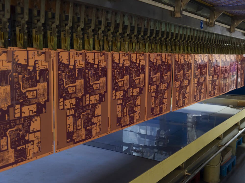
Step 3: Print the Copper for the Interior Layers
This step is the first step in the process where the PCB manufacturer starts to develop the PCB. After the PCB design is printed on a piece of laminate, copper is then pre-bonded to that same piece of laminate, which assists in the structure of the PCB. The copper is then imprinted away to reveal the blueprint from earlier.
Next, the laminate panel is covered by a type of photo-sensitive film called the resist. The resist is made of a layer of photo-reactive chemicals that harden after they’re exposed to ultraviolet light. The resist allows technicians to get a perfect match between the photos of the blueprint and what’s printed on the photo resist.
When the resist and the laminate are lined up using the holes from earlier, they receive a blast of ultraviolet light. The ultraviolet light passes through the translucent parts of the film, hardening the photo resist. This indicates areas of copper that are meant to be kept as pathways. In contrast, black ink prevents any light from getting to the areas that aren’t meant to harden so that they can later be removed.
Once the board has been prepared, it is washed with an alkaline solution to remove any of the leftover photo resist. The board is then pressure-washed to remove anything left on the surface and left to dry.After the drying process, the only resist that should be left on the PCB is on top of the copper that remains as part of the PCB when it’s finally popped free. A technician looks over the PCBs to make that there are no errors. If no errors are present, then it’s on to the next step
Step 4: Avoid the Unneeded Copper
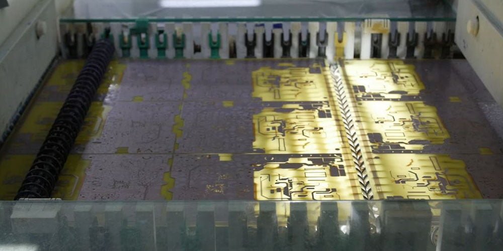
The next stage in the PCB manufacturing process is of removing unwanted copper. Much like the alkaline solution from earlier, another powerful chemical is used to eat away at the copper that is not covered by photo resist. Once the unprotected copper is removed, the hardened photo resist from earlier needs to be removed, as well.
Note: When it comes to removing the unwanted copper from your PCB, heavier boards may require more exposure to the solvent or more copper solvent.
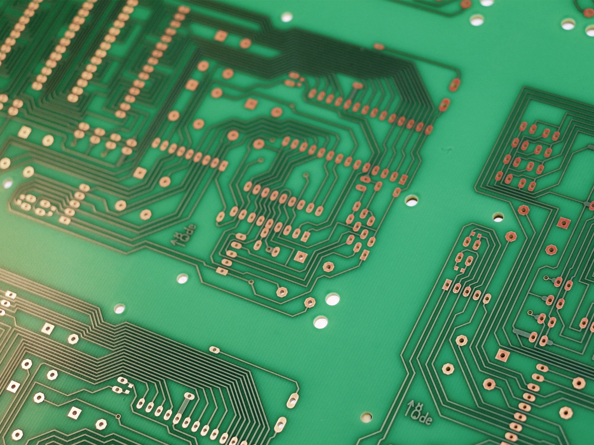
Step 5: Inspection and Layer Alignment
After PCB’s layers have been cleaned individually, they are ready for an optical inspection and layer alignment. The holes from earlier are used to align the outer and inner layers. A technician places layers on a type of punch machine known as an optical punch to align the layers. Then optical punch drives a pin down through the holes to array the layers of the PCB.
After the optical punch, another machine performs an optical inspection to make sure there are no faults. This optical inspection is incredibly important because once the layers are placed together, any errors that exist can’t be corrected. To confirm that there are no faults, the AOI machine compares the PCB to be inspected with the Extended Gerber design, which serves as the manufacturer’s model.
After the PCB has passed inspection — that is, neither the technician nor the AOI machine found any defects — it moves onto the last couple steps of PCB manufacture.
Step 6: Laminate the PCB Layers
At this in the PCB manufacturing process, the PCB layers are all together, waiting to be laminated. Once the layers have been confirmed as being defect-free, they’re ready to be fused together. The PCB laminating process is done in two steps: the lay-up step and the laminating step.
Outside of the PCB are finished pieces of fiberglass that have been pre-coated/pre-soaked with an epoxy resin. The original piece of the substrate is also covered in a layer of thin copper foil that now contains the etchings for the copper traces. Once the outer and inner layers are ready, it’s time to push them together.
The insertion of these layers is handled using metal clamps on a special press table. Each layer fits onto the table using a specialized pin. The technician doing the laminating process starts by placing a layer of pre-coated epoxy resin which is known as pre-impregnated or prepreg. In the alignment basin of the table. One individual layer of the substrate is placed over the pre-impregnated resin, followed by a layer of copper foil. The copper foil is in turn followed by more sheets of pre-impregnated resin, which are then finished off with a piece and one last piece of copper known as a press plate.
Once the copper press plate is in place, the stack is ready to be hard-pressed. The technician takes it over to a mechanical press and presses the layers down together. As part of this process, pins are then punched down through the stack of layers to make sure that they are fixed properly.
If the layers are fixed correctly, the PCB stack is taken to the next press, a laminating press. The laminating press uses a pair of heated plates to apply both pressure and heat to the stack of layers. The heat of the plates usually melts the epoxy inside of the prepreg. This and the pressure from the press combine to fuse the stack of PCB layers together.
When the PCB layers are pressed together, there is a little bit of unpacking that needs to be completed. The technician needs to remove the pins and top press plate from earlier, which then allows them to pull the actual PCB free.
Step 7: Drilling
Before the process of drilling, an X-ray machine is used to locate the drill spots. Then, guiding/registration holes are drilled so that the PCB stack can be protected before the more precise holes are drilled. When the time comes to drill these holes, a computer-guided drill is used to make the holes, using the file from the design as a guide.
Once the drilling is complete, any additional copper that’s left over at the edges is filed off.
Step 8: PCB Plating
After the panel has been drilled, it’s ready to be plated. The plating process uses a chemical to fuse all of the different layers of the PCB together. After being cleaned thoroughly, the PCB is bathed in a series of chemicals. Part of this bathing process coats the panel in a micron-thick layer of copper, which is deposited over the topmost layer and into the holes that have just been drilled. Before the holes are completely filled with copper, they simply serve to expose the fiberglass substrate that makes up the panel’s insides. Bathing those holes in copper covers the walls of the previously drilled holes.
Step 9: Imaging and Plating of the Outer Layer
Earlier in the process (Step number 3), a photo resist was applied to the PCB panel. In this, it’s time to apply another layer of photo resist. However, this time the photo resist is only applied to the outside layer, since it still needs to be imaged. Once the outer layers have been coated in photo resist and imaged, they’re plated in the exact same way the interior layers of the PCB were plated in the previous step. However, while the process is the same, the outer layers get a plating of tin to help guard the copper of the outside layer.
Step 10: The last Etching
When it comes time to etch the outside layer for the last time, the tin guard is used to help protect the copper during the etching process. Any undesirable copper is removed using the same copper solvent that was mentioned earlier, with the tin protecting the valued copper of the etching area.
Once all the unwanted copper is removed, the PCB’s connections have been properly established and it’s ready for solder masking.
Step 11: Apply the Solder Mask
To make the panels completely ready for solder mask application, they are to be cleaned. When the PCB panels have been cleaned, an ink epoxy is applied along with a solder mask film. Then boards are blasted with ultraviolet light to mark out certain portions of the solder mask for removal.
After the unneeded pieces of solder mask have been completely removed, the PCB is placed into an oven and heated so that the solder mask will cure.
Step 12: Finish the PCB and silk screening
As part of the finishing process, the PCB is plated with silver, gold, or HASL so that the components are able to be soldered to the pads created and protect the copper.
After the PCB has been silver or gold plated, as essential, it is silk-screened. The silk-screening process prints all of the active information on the PCB, such as company ID numbers, manufacturer marks, and warning labels.
Once the PCB has been plated & silk-screened with the correct information, it can be sent along to the final curing stage.
Step 13: Electricity Reliability Testing
After the PCB has been coated and cured (if necessary), a technician performs a battery of electrical tests on the different areas of the PCB to ensure functionality. The main tests that are performed are isolation tests and circuit continuity. Circuit continuity test checks for any interruptions in the PCB, known as “opens.” The circuit isolation test, on the other hand, checks the isolation values of the PCB’s various parts in order to check if there are any shorts. While the electrical tests mainly exist to make sure functionality, they also work as a test of how well the initial PCB design stood up to the manufacturing process.
There are other tests that can be used to determine if a PCB is completely functional. One of the few main tests used to do this is known as the “bed of nails” test. During this test, numerous spring fixtures are attached to the test points on the circuit board. The spring fixtures then subject the test points on the circuit board with up to 200 grams of pressure to see how well the PCB stands up to high-pressure contact at its test points.
If the PCB has completely passed its electrical reliability testing and any other testing the manufacturer chooses to implement it can be moved on to the next step: cutting.
Step 14: Cutting and Profiling
The final step of the PCB manufacturing process is the cutting and scoring of the PCB. This involves cutting out the different PCBs from the original panel. There are two ways that PCBs can be cut from their original panels:
Using a V-groove, which cuts a diagonal channel along the sides of the board
Using a router or CNC machine, which cuts out small tabs around the edges of the PCB.
Either way, your PCB will be able to easily come free of the construction paneling.
Normally, PCB panels have larger arrays or individual boards, if applicable, scored and routed out so they can be broken off from the construction board after they’ve been assembled.
When the boards are broken off from the construction board, there is a final inspection phase of PCB manufacture:
The boards are checked over for general cleanliness to ensure that there are no sharp edges, burrs, or other manufacturing hazards
A visual inspection can be directed, if essential, to make sure that boards meet industry specifications and match up to the details laid out in the data: the technician can also use the visual inspection to verify the physical dimensions and the hole sizes of the PCB if needed.
Slots, chamfers, bevels, and countersinks are added during the routing and fabrication process, as necessary
If possible, any shorts are repaired — the shorted boards are then re-tested using the same electrical reliability tests from above.
Choose MOKO Technology for PCB Manufacturing Service
As listed above, there are many steps involved in PCB manufacture, each step must be executed correctly to ensure the high quality of the product, any slight mistake could impact the performance of circuit boards. Therefore, if you are not well-versed in PCB manufacture, you can choose to outsource PCB manufacturing services to a reliable PCB manufacturer. MOKO Technology, with years of experience in the industry, has become a leader in providing PCB manufacturing services that meet the needs of customers across various industries. Our state-of-the-art facilities, advanced PCB fabrication technology, and experienced team ensure that each PCB produced is of the highest quality and meets the strictest standards. Additionally, we offer a range of customization options to cater to the specific needs of each customer. Contact us to start your PCB manufacturing project now!