High density PCB construction
High-density ICs force high density PCB designers to find new design strategies to either have more functionality on smaller plates – in end-user products – or much more function on larger parts.
Another generation of smaller elements on integrated circuits is on the way. This is in the 65 nm range, but some IC manufacturers are already developing prototypes with 45 nm elements. The smallest elements in currently produced ICs, about 90 nm, already conflict with the physical basis of the connection.
Printed connections, or tracks, can only be small until signal integrity and performance distribution problems occur on the disk. The assembly of the new chips on each plate type will require both some new strategies as well as those used in the past.
These problems in the design of printed circuit boards are known: receiving signals from ICs and sending them to ICs, maintaining signal integrity, and distributing power to the components of the disk. Signal integrity means avoiding crosstalk, which occurs when traces are too close to each other, and managing impedance to avoid signal reflections that are more likely to occur in too long a track because they occur on very large high density PCB plates.
There is also a new complication: very short rise and fall times. Then, even with very short tracks, potentially additional impedance problems may occur.
Five years ago, a Terabit Internet router was a top product. It contained 52 PCBs and was half a rack or 3 feet high, 2 feet deep and 18 inches wide. Now the router has only one PCB and is only 1.5 inches high. If we had been told at the time that an IC could house billions of transistors and 10 Gbps-compatible tracks, we would have laughed. Now I don’t know if there are any size and speed limits at all.
The signal integrity issues on disks with smaller ICs and tracks can often be handled with familiar techniques: managing track size and separation to minimize crosstalk and construct track connections with appropriate resistors to avoid reflections. We consider thousandths of an inch as minimum track width, and 7 to 8 thousandths of an inch as the minimum distance between them, no matter how many pins a chip has. He prefers a separation of 10-thousandths of an inch.
New PCB Architectures
The design of high density PCB has taken two paths. One leads to the PCBs that are really high-density, used in mobile phones, digital cameras, and other consumer and home electronics devices, where all circuits fit on a thumb-nail sized board and power must be distributed sparingly to extend the service life between individual charges. The other leads to high-performance PCBs in supercomputers, extreme high-speed routers, and similar systems.
On these tiny PCBs, PCB designers don’t have to squeeze components in confined spaces, but performance with low power requirements is everything. Larger PCBs operate at very high speeds. The two types of high-density disks have different problems, while designers scale down to the next generation of ICs with smaller elements.
For high-performance disks with ICs that have 1,000, 2,000, or even more pins, the physical limits imposed by standard connections probably require radically different design techniques.
One example, a self-proclaimed signal integrity evangelist whose company, be The Signal, is located in Olathe, Kansas, is a cube-shaped 3-D PCB.
This is not a collection of stacked layers. It’s an integrated design that’s specific to 3-D, where all important processes run vertically across multiple layers of processors.
Other techniques focus on laminates. Manipulation of laminate material can help reduce signal loss, and very thin plates can support shorter and more connections. Some new production laminates are only 2 thousandths of an inch thick and become thinner. According to Bogatin, these laminates can allow designers to halve the number of layers in a PCB while improving performance provision.
Operating speeds of high density PCB increased from 10 to 20 MHz in the 1980s to gigabit-per-second in the 21st century. In the 1980s, you could design a plate with your eyes closed. Now you have to open both eyes wide.”
Simulation and training
As the panels become more complex and their manufacturers don’t want to waste 1,500-pin ICs due to poor design, simulation and modeling are critical to PCBs. If something doesn’t work, you need to take qualified action, and you can’t get on with tried-and-tested rules of thumb. Disks are increasingly similar to ASICs [Application Specific Integrated Circuits], and now we increasingly need the same type of simulation as for as ICs. Simulation tools that generally do this are now available, but performance integrity toolsets are still missing today.
Extremely high density PCB
MOKO Technology shows the technology platform Dencitec, which allows an extremely high density of integrated functions for printed circuit boards with high throughput.
These options include conductor and spacing widths of up to 25 μm with copper thicknesses of 20 ± 5 μm on all conductive layers, laser via diameter of 35 μm, residual rings with a diameter of 30 μm on the inner layers and 20 μm on the outer layers, copper-filled blind vias with the possibility of via stacking and vias in pads. This leaves more space for the integration of additional options such as energy supply (batteries, etc.). In addition, modern materials enable the manufacture of ultra-thin circuits, such as four-layer flex circuits with a total thickness of less than 120 μm. In contrast, commonly used standard processes only deliver good results up to conductor widths and spacings of 50 μm and classic semi-additive processes such as thin-film technology enable conductor widths and spacings of less than 15 μm, but are generally limited to production formats.
A simulation of the galvanic copper deposition in the PCB production
Before we produce a high density PCB board, we carefully analyze the data received. This is how we find all potential effects on production, which could impair quality and long-term reliability.
Until now, electroplating has been a field in which hardly anyone has been able to determine exactly how a particular design will behave. The copper layer thickness that is deposited on the circuit board depends on the layout density. If the density is low, we risk building too much; if the density is high, we risk too little build-up. A copper structure that is too strong means that the holes in the holes become too small. A copper structure that is too low means that the hole walls are too weak, so that the plated-through holes can break during assembly and lose their long-term reliability.
The goal is a uniform copper density and a uniform structure over the entire circuit board. We take this into account as much as possible when placing the printed circuit boards on our production benefits. We can place additional copper patterns (so-called compensation surfaces) between and around the circuit board to compensate for the density. Nevertheless, we are limited to these methods because we cannot modify the actual design of the circuit board. Only the developer can do this.
Historically, there have been no developer tools to determine copper density. Today MOKO Technology offers a solution with a color-coded image of the printed circuit board, which shows the potential areas of the superstructure and substructure of copper.
We use special galvano-simulation software that divides the board into small cells. The copper density of each cell is compared to the average copper density of the entire circuit board and color is then assigned to this cell. A copper density lower than average is colored on a scale from green (average), yellow and orange to red. The more red, the lower the relative density and the higher the risk of excessive copper build-up in this area. Cells with a higher copper density are colored on a scale from green to dark blue. The more blue, the greater the risk of insufficient copper build-up.
Armed with this visual data, the developer can add copper areas in low-density areas or reduce large copper areas.
In addition, we will provide a galvano index that measures the uniformity of the copper density on the circuit board. A completely uniform circuit board has an index of 1. This means that no electroplating problems are to be expected. Lower values show less uniformity and are highlighted on the visualized image by red and blue areas. If the index falls to 0.8 or less, special attention is required. In the example shown above, the galvano index is 0.65. The blue area, which is too small, can be clearly seen.
The galvano picture is created when a new order is placed. This galvano picture is part of “PCB Image”, a realistic representation of your printed circuit boards, which we will send you together with the order confirmation. In the near future, this simulation will become part of the price request function. We will do a number of checks and create a report from them. Based on the galvano picture, which was also created, the designer can see whether he can make changes to improve the uniformity of his high density PCB circuit board.
After the modification, the galvano index is 0.95. The picture shows a uniform copper deposition.
Galvano simulation – good galvano index layer pattern – good galvano index
Of course, there may be design restrictions that make a less uniform copper density unavoidable. For this, we are preparing another solution to improve the quality and reliability of the finished printed circuit board. The Elsyca Intellitool anode matrix project will further improve the uniformity of the final copper structure.
More packing density for complex electronics
The high density PCB boards have to keep up with the advances in microchips. Circuits with a high packing density represent a technological leap, which should have as far-reaching consequences as the transition to surface mounting in the mid-eighties.
Progressive miniaturization of components, chips, and systems will mean a drastic technological leap for printed circuit board manufacture in the coming years as well as due to the introduction of surface mounting (SMT) in the mid-eighties. The highest growth rates are currently to be expected in the field of high-tech circuits because the integration success of the microchips means that the connection technology is also required. The challenge is to produce the finest structures for printed circuit boards with high integration density (High Density Interconnection – HDI) economically.
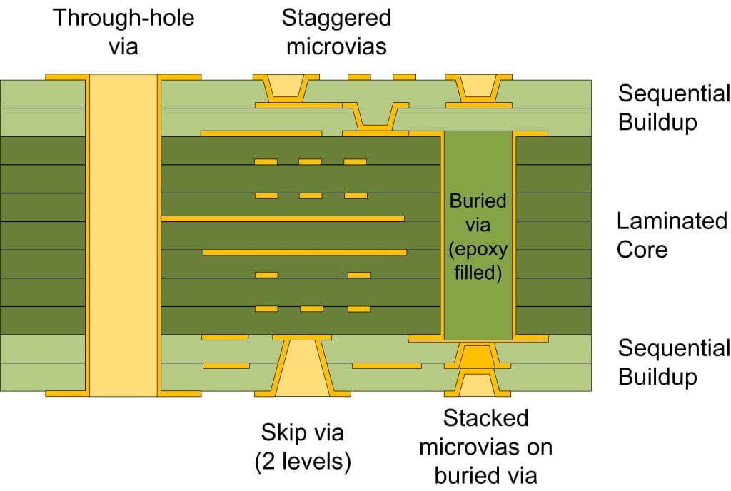
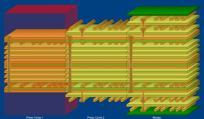
So far, the contacting problems with multi-pole components have been solved by moving some of the connections to one or more additional signal layers. However, the production of multilayer circuits (multilayer) is comparatively complex and therefore costly. However, the number of layers can generally only be reduced by using finer conductor pattern structures or by using smaller hole diameters. In order to electronically connect the individual signal layers of the circuit board to one another, the conductor tracks are so-called vias, i. H. drilled and then metalized holes, led to the next level or the underside of the plate. Since a printed circuit board can have several thousand holes, there is enormous potential for savings simply by reducing the hole diameter. Mechanically, however, such micro-holes (micro vias) with a diameter of less than 0.1 mm can only be produced with lasers, whereas traditional drilling at 0.2 mm reaches its limits.
However, micro vias are only the first step towards even more complex circuits in fine-wire structuring. The particularly critical work steps here include the entire photo process, with the help of which the copper cladding of the circuit board base material is usually structured. The ultra-fine conductor technology places particularly high demands on the exposure and on the subsequent etching step. If structures with a width and spacing of less than 0.1 mm are to be realized in series production, the production yield drops dramatically in some cases. This can be remedied by new production methods that significantly simplify the entire photo process. This includes direct laser exposure, which describes the photoresist directly with the conductor pattern. The conventional exposure step using a film is completely eliminated.
Technically, direct exposure is superior to previous contact exposure because it offers more flexibility with regard to lot sizes and a higher structure resolution. The number of process steps can thus be significantly reduced. Running costs for clean room, films and masks, photoresists as well as the resulting expenses for the disposal of environmentally harmful materials and residues are also reduced with this procedure. Higher yields can be achieved especially with very fine conductors since the high coherence of the laser beam enables reliable imaging of the smallest structures with minimal under-radiation. And due to the higher depth of field of the direct imagesetter, even differences in height can be compensated to a certain extent. Automatic optical panel measurement and individual usage indicators are also conceivable as additional functions. Laser direct structuring is even easier, in which the laser mills the conductor pattern directly into the copper cladding, which means that a resist is no longer required.
Chinese companies are also leaders in the development of new connection technologies. “MOV” from the Karlsruhe company Inboard is a new concept and stands for multi-layer surface wiring. This new type of high density PCB circuit board is also called an “integral circuit board” because electronic components such as resistors and capacitors are integrated into the circuit board.
The integrated circuit board not only offers finer conductor track structures and laser-drilled blind holes of less than 80 µm in diameter for contacting the conductor tracks, but the electrical data are also impressive. Compared to conventional multi-layer wiring, the cable length with the same function is reduced by 35%. The number of vias through all layers is even reduced by 80%, the number of signal layers in a reference example from six to only two.
But it is important that you can get by with one-sided assembly technology again. Resistors and capacitors can be included as “printed” components. This new development was triggered by the increasing demands on the working frequency, the number of component connections and ever-smaller designs such as ball grid array and chip size packaging. For example, with 50 printed resistors on a printed circuit board, there is a cost advantage over SMD assembly, according to the inboard.
We are working on cost-effective solutions for optical data transmission. A strip-shaped optical fiber made of plastic, which is attached to a so-called backplane, connects hardware components in the computer via very flat, light-conducting plastic strips of up to 50 cm in length. The novel manufacturing process for the strip waveguide is suitable for any carrier materials, in particular for printed circuit board material. We take a different approach and integrates the optical conductors produced by hot stamping into special circuit board layers. This enables passive optical components such as branches to be implemented, which allow optical wiring analogous to electrical circuit board technology. The circuit board is evolving from a simple connecting element to a complex assembly.