Increase The Integration Density of PCB by filling blind microvia and through holes using electrolytic copper deposition.
The progressive miniaturization of electronic circuits increasingly requires the use of HDI circuit boards with copper-filled blind microvias. A newly developed copper electrolyte, which is currently being tested under production-related conditions, enables defect-free filling of blind microvias with a small copper layer thickness on the circuit board surface. A copper electrolyte currently in development should also enable the reliable filling of through holes in the future – the current development work is already showing promising results.
Filling of Blind Microvia and Through-holes
Increasing the Packaging Density of PCBs by Filling of Blind Micro-vias and Through-holes by Electrodeposition of Copper.
The increasing miniaturization of electronic circuits makes the use of HDI PCB (HDI printed circuit boards) with copper-filled blind micro-vias, increasingly desirable. A newly-developed copper electrolyte, currently under test in simulated production conditions, will enable defect-free filling of blind micro-vias while at the same time allowing reduced copper deposit thickness on the board surface. This brings with it a more efficient use of materials her and thus a reduction in the cost of PCB manufacture. Another copper electrolyte now under development promises to allow a reliable filling of through-holes.
1 Introduction
In microelectronics, there is still a trend towards miniaturization, that is, towards smaller and more powerful systems that are also supposed to be less expensive than previous systems. The best-known examples of this are smartphones and tablet PCs, the performance of which – in spite of the same or even smaller device size – has increased significantly in recent years.
HDI printed circuit boards (HDI: High-Density Interconnect) make a significant contribution to miniaturization. For the electrical connection of individual PCB layers, space-saving blind holes (blind microvias) are used instead of through holes. The integration density can be further increased by filling the blind microvias with electrolytically deposited copper (blind microvia filling). In the meantime, the use of HDI circuit boards is no longer restricted to mobile electronics but is also increasingly being used in other applications, for example in the automotive sector.
A newly developed electrolyte, which in the Blind Microvia Filling only deposits a very small layer thickness of copper compared to the previous generation of electrolytes, enables the resource, energy and cost-efficient production of HDI printed circuit boards.
Since the integration density of HDI printed circuit boards can be increased even further by using very thin core materials, the development of electrolytes for filling through-holes (English: Through Hole Filling) is currently being strengthened. Results of the development work in this area are presented.
2 Miniaturization in the field of microelectronics
The best-known representatives of the progressive miniaturization in microelectronics are very powerful mobile devices such as smartphones and tablets. The high and constantly growing sales figures reflect the great attractiveness of these devices. In 2013, more than 1 billion smartphones were sold for the first time, sales of around 1.2 billion are expected in 2014 and around 1.8 billion in 2017 [2]. In the area of tablet PCs, sales of 271 million devices are predicted for 2014, which corresponds to an increase of almost 40% compared to the previous year [3].
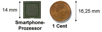
These are installed in processors with very small housing sizes and a very large number of increasingly grid-like connections. The underside of the processor has 976 connections on an area of just under 2 cm², this corresponds to around five connections per square millimeter. The pitch of the connections is only 400 µm.
3 Miniaturization in the area of printed circuit boards
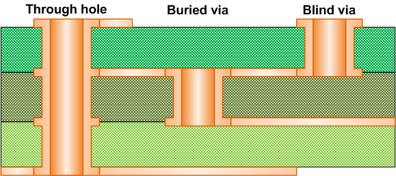
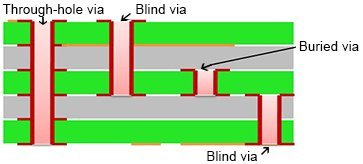
Printed circuit boards with a correspondingly high integration density are required for space-saving and reliable electrical connection of processors with extremely high connection densities. The classic multilayer printed circuit board is unsuitable for this, however, since it uses through holes for the electrical connection of individual printed circuit board layers. These have relatively large diameters and, since they are drilled only after the individual layers have been pressed, they extend over the entire circuit board thickness. The consequence of this is that even when directly adjacent layers are connected, the space above and below the actual connection is lost and therefore cannot be used for other structures, for example conductor tracks. The resulting low integration density of multilayer circuit boards is not sufficient for the requirements described above.
A few years ago, a new, highly integrated generation of printed circuit boards, the so-called HDI circuit board, was therefore developed, which was initially used primarily for the production of mobile phones. When manufacturing HDI printed circuit boards, the individual printed circuit board layers are built up successively (SBU, Sequential Build Up). The electrical connection of adjacent assembly positions is realized using laser-drilled blind microvias. Figure 2 shows schematically the structure of a 2-4-2 HDI circuit board, i.e. the circuit board consists of a four-layer multilayer core and two layers on each side.
4 Blind microvia
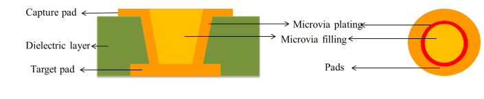
Compared to through holes, blind microvias have smaller diameters in the range from 50 µm to 150 µm and they only extend in the z-direction over the thickness of a mounting position (typically 50 µm to 150 µm). They only take up as much space as is actually required for the actual connection. HDI printed circuit boards thus have a much higher integration density than multilayer printed circuit boards and are therefore suitable for the signal unbundling of highly functional electronic components in the smallest space.
4.1 Filling blind microvia
A further increase in the integration density enables stacked blind microvias (stacked blind microvias). If electrolytically deposited copper is used for filling instead of conductive paste, this leads to the following further advantages:
Increased reliability (the blind microvias only contain copper, there is no additional interface)
better heat management (heat loss can be dissipated via the highly heat-conductive, copper-filled blind microvias)
Further increase in integration density (no additional pads (pads) are required on the circuit board surface for contacting components)
The main process steps in the manufacture of HDI circuit boards with copper-filled blind microvias are shown schematically in Figure 4. If a further layer is to be built up, the process sequence must be run through again starting with process step 2.
Stacking copper-filled blind microvias on top of each other means that even non-adjacent assembly positions can be connected in an electrically conductive manner with minimal space requirements (Fig. 5). The use of pad-in-via or via-in-pad designs leads to a further increase in the integration density, since component connections can be soldered directly onto the copper-filled blind microvias, so that no additional connection surfaces are necessary (Fig. 6).
4.2 Previous electrolytes for blind microvia filling
Typically, electrolytes for blind microvia filling contain a relatively high concentration of copper ions in the range from 40 g / l to 60 g / l in combination with a low sulfuric acid concentration in the range from 10 ml / l to 50 ml / l as well as chloride ions. The organic electrolyte additives required to control the coating properties differ from specialist company to a specialist company, but mostly the following three components are contained in the electrolyte additives:
Basic additive (inhibitor)
Grain Refiner (Activator)
Leveler (inhibitor)
In addition, the methods of the different providers can also differ in the following features:
System technology (standard vertical system, vertical continuous system, horizontal continuous system)
Anode type (copper anode, insoluble anode)
Current form (direct current, pulse current, reverse pulse current)
applicable current density
The methods previously offered by Schlötter for blind microvia filling work exclusively with direct current in standard vertical systems or vertical continuous systems.
In the early years of blind microvia filling, there were essentially the following additional requirements in addition to the standard requirements for electrolytically deposited copper coatings for printed circuit boards (e.g. ductility, reliability):
defect-free filling of the blind microvias without electrolyte inclusions
Minimum filling level or maximum allowed deepening (dent.
During the filling process, 93 µm copper (B) was deposited in the blind microvia, while the layer thickness on the surface is only 22 µm (C), resulting in the following key figures:
Indentation (A-B): 30.4 µm
Degree of filling (B / A): 75%
Metal distribution (B / C): 426%
It is primarily due to the mode of action of the leveler, by means of which the copper is not deposited on the surface but rather in the blind microvias, i.e. in the areas of low current density and low electrolyte exchange.
To achieve a good filling result, the electrolyte additives must be very well coordinated. Figure 8a shows a blind microvia before the filling process as well as different results, which can only occur through variation of the electrolyte additives – with otherwise the same separation parameters (Fig. 8b – e).
4.3 New electrolyte for blind microvia filling
The integration density of the circuit boards can be increased even further by reducing the track width and spacing. For the etching of such fine conductors, however, the copper layer thickness on the surface must be low, since otherwise severe undercutting and problems with the conductor cross-section can occur.
As shown in Figure 4, the copper layer thickness can be reduced after filling with – possibly repeated – copper thinning, but additional process steps and systems are necessary for this. In addition, copper thinning of copper that was previously deposited is partially removed, which has a negative impact on resource, energy and cost efficiency in the manufacture of printed circuit boards. To completely avoid – or at least to reduce – the copper thinning, in addition to the requirements already mentioned, the requirement to deposit the smallest possible copper layer thickness during the filling process has been added in recent years.
50-70 mg / l chloride
3–10 ml / l additional slotocoup SF 31
0.2–1.0 ml / l additional slotocoup SF 32
0.2–2.0 ml / l additional slotocoup SF 33
The electrolyte is operated at current densities of maximum of 2 A / dm² in the temperature range between 18 ° C and 22 ° C.
Compared to the previous generation of electrolytes, the copper layer thickness deposited on the surface could be extremely reduced. This is shown by the metal distribution, which in the laboratory test shown has an extremely high value of over 2000% (Fig. 9b).
Slotocoup SF 30 is currently being tested in cooperation with the Taiwanese Schlötter partner AGES in the PCB Development Center in Taipei opened in 2012 under production-related conditions in a 7200 liter vertical continuous system (Fig. 10).
Deepening: 7.0 µm
Degree of filling: 91%
Metal distribution: 740%
Figure 11b shows another copper-filled Blind Microvia, which comes from the same circuit board as the Blind Microvia in Figure 11a. It is noteworthy that, despite the non-optimal BMV geometry, the filling result is very good.
Slotocup SF 30 also enables defect-free filling of closely spaced blind microvias with a low layer thickness of the copper surfaces.Fig. 12: Slotocoup SF 30 test results when filling closely spaced blind microvias
Very flat blind microvias, which result when extremely thin dielectrics are used, can also be filled defect-free with the new electrolyte, but this results in somewhat higher copper layer thicknesses.
5 Through-Hole Filling
A further increase in the integration density of HDI printed circuit boards can be achieved by replacing the relatively thick multilayer cores that have been used up to now with significantly thinner cores with thicknesses between 100 µm and 200 µm.
Very thin cores can also have through holes instead of blind microvias. Previously, these through-holes were first filled with paste after the first copper plating and then copper-plated again to produce the pads. In addition, the use of paste can lead to reliability problems.
5.1 New electrolytes for through-hole filling
Initially, attempts were made to use the copper electrolytes that had already been tried and tested in blind microvia filling in the area of through-hole filling. However, it was shown that these electrolytes are not suitable for this application so that further development work was necessary. Some laboratory results from the current development work are shown in Figure 16.
By modifying the electrolyte composition, it was possible to significantly improve the filling of through holes (approx. 85 µm borehole diameter / approx. 110 µm borehole depth). All four depositions shown in Figure 16 were each carried out with direct current with the same deposition time and current density. In addition, only one electrolyte was deposited during the entire deposition period, i.e. there was no electrolyte change in the course of the deposition.
With increasing aspect ratio, i.e. decreasing borehole diameter and / or increasing borehole depth, the mass transport and thus the subsequent delivery of copper ions is made more difficult. As a result, defect-free filling of the through-holes without electrolyte inclusions is becoming increasingly difficult. Figure 17 shows two filling results of non-preamplified through holes (approx. 50 µm borehole diameter / approx. 160 µm borehole depth).
The electrolyte enclosed in the defect (Fig. 17a) expands when the HDI circuit board is heated and can therefore already lead to a crack in this connection during the soldering of components or when the temperature is subsequently increased, which can lead to a system failure. The focus of the current development work is, therefore, the reliably defect-free filling of through-holes with different aspect ratios.
6 Inconclusion
Due to their high integration density, HDI printed circuit boards enable reliable unbundling of the high connection densities of these microprocessors in the smallest space.
By filling blind micro vias with electrolytically deposited copper, the integration density of HDI printed circuit boards can be further increased. The newly developed electrolyte Slotocoup SF 30, which is currently being tested in Taiwan under production-related conditions, enables defect-free filling with a low copper layer thickness. This leads to a further increase in the integration density and to a more resource, energy and cost-efficient production of HDI printed circuit boards. The first installation at a customer is scheduled for the second quarter of 2014.
The integration density can be increased even further by means of so-called coreless structures, which consist of very thin core materials. Results of current development work show that direct current deposition of copper makes it possible in principle to fill the through holes in these cores. Since the filling result and thus the quality of the connection depends on the aspect ratio of the through-holes, the realization of a reliable defect-free filling with different aspect ratios is currently in the foreground of the development work.