There are many challenges in the design and manufacture of PCBs, one of which is to ensure signal integrity and high-speed data transfer rates, which are critical for high-frequency PCBs. It is worth mentioning that PCB back drilling can effectively solve this problem. In this article, we aim to give you a thorough overview of the back drilling technique, covering its definition, benefits, the step-by-step process, and so on. Let’s just dive right in…
What Is PCB Back Drilling?
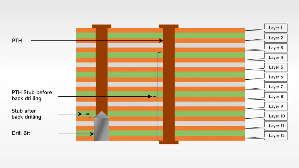
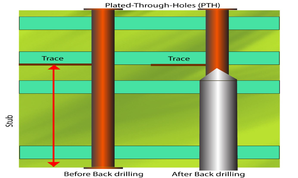
The process of PCB back drilling, also referred to as controlled depth drilling, involves removing the stub in multilayer PCBs to create vias. The aim of back drilling is to facilitate the flow of signals between different layers of the board without interference from unwanted stubs.
When to Use Back Drilling?
It is generally recommended to consider adding the technique when the circuit track on the PCB board with a frequency range between 1GHz and 3GHz . However, designing high-speed interconnection links is a complex system engineering task, and other factors such as the chip’s drive capability and the length of the interconnection links should also be considered. Therefore, the system interconnection link simulation is the most dependable approach to determine whether back drilling is required or not.
PCB Back Drilling Example
To provide a clearer explanation of the back drilling process, let’s consider an example. Suppose there is a 12-layer PCB with a through-hole connecting the first and 12th layers. The aim is to connect only the first layer to the 9th layer, while keeping the 10th to the 12th layers unconnected. However, the unconnected layers create “stubs” that can interfere with the signal path, resulting in signal integrity problems. Back drilling involves drilling out these stubs from the reverse side of the board to improve signal transmission.
Why Is Back Drilling Needed in PCB Fabrication?
- Back drilling helps to reduce signal attenuation, ensuring a stronger and more reliable signal. Additionally, this technique helps to minimize the impact of stubs on impedance matching, which in turn reduces EMI/EMC radiation.
- Back drilling is also an effective way to prevent signal distortion issues. Via stubs are well-known for causing deterministic jitter, which can result from signal crosstalk, EMI, and noise. By removing these stubs, back drilling can help to eliminate the sources of deterministic jitter, improving signal quality and preventing signal distortion issues.
- Back drilling helps to minimize crosstalk between vias.
- By implementing back drilling, the deterministic jitter in your signal can be reduced, which can result in a decrease in the overall bit error rate (BER)of the signal.
- Reduced excitation of resonance modes. l
- Minimize the usage of buried and blind vias to simplify PCB production.
- Minimal impact on design and layout.
- Expanded channel bandwidth;
- Lower costs can be achieved compared to sequential laminations.
How Back Drilling Works?
There are 5 key steps involved during the PCB back drilling process, below is a detailed breakdown of each step:
Step 1: Initial Drilling
First, drill a plated through-holes (PTHs) to create electrical connection among different layers of the board. Then plate the hole with copper to achieve conductivity between the required layers.
Step 2: Identification of Via Stubs
Analyze the PCB design and determine whether vias contain a stub that is not needed. Such subs would affect the signal integrity and cause the signal degradation.
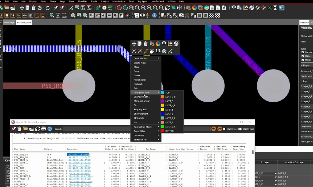
Step 3: Back Drilling Setup
Before start the back drilling, it’s critical to setup a CNC drilling machine to ensure precise control. Additionally, the selection of drill bit also matters. It should slightly larger than the hole diameter, usually 0.1-0.2mm.
Step 4: Back Drilling Process
In this step, PCB would be fixed into the CNC machine firmly, and the machine drills from the opposite side of the board. This process can remove the excess stub portion of the via without damaging the surrounding structure.
Step 5: Cleaning and Inspection
Once the back drilling is done, the PCB should be cleaned to remove residual debris, such as drill chips or copper particles. Finally, check the back-drilled holes to verify if they are drilled with correct depth and diameter.
Top 6 Design Tips for PCB Back Drilling
- To ensure proper back drilling, it is necessary to provide the PCB board manufacturer with separate output files containing the back-drill layers, along with the specifications detailing which layers require corresponding back drilling.
- The diameter of the back drilling holes should be at least 0.2mm larger than the diameter of the first drill holes, and the distance between the back drilling through the layer and the trace should be 0.35mm for the first drill and 0.2mm for the back drilling.
- During PCB stack-up design, the dielectric thickness should be considered to avoid drilling into traces that should not be drilled. If drilling is required for a specific layer (such as layer “L”), the dielectric thickness between the adjacent layers that do not require drilling and layer “L” should be at least 0.2mm.
- To optimize the back drilling process, it’s important to minimize the number of via stubs and avoid blind vias.
- Placing vias in less critical areas and maintaining a minimum distance between back drill holes and signal traces can also help prevent signal reflection and other issues.
- Keeping back drill hole diameters small is important to avoid damaging traces and planes lateral to the backboard hole.
Challenges of Back Drilling Process
- Back drilling depth control
Controlling the depth of back drilling is essential for processing blind vias accurately. The tolerance of back drilling depth is mainly influenced by the accuracy of the back drilling equipment and the medium thickness tolerance. However, external factors such as the drill’s resistance, drill tip angle, contact effect between the cover board and measuring unit, and board warpage can also affect the accuracy of back drilling. During production, it’s important to select appropriate drilling materials and methods to achieve the best results and control the accuracy of back drilling. By carefully controlling the depth of back drilling, designers can ensure high-quality signal transmission and prevent signal integrity issues. - Back drilling accuracy control
Accurate control of back drilling is crucial for the quality control of PCB in subsequent processes. Back drilling involves secondary drilling based on the hole diameter of the primary drill, and the accuracy of the secondary drilling is critical. Several factors, including board expansion and contraction, equipment accuracy, and drilling methods, can affect the accuracy of the secondary drilling coincidence. Therefore, it’s important to ensure precise control of the back drilling process to minimize errors and ensure optimal signal transmission and integrity.
Conclusion
As an important method to ensure PCB signal integrity, back drilling is widely used in the PCB manufacturing process. Hope you can better understand and use this technology after reading this blog. If you have other questions, you can contact us and talk to one of our experts. As a leading PCB manufacturer in China, MOKO Technology has all the PCB expertise and skills needed to help you.