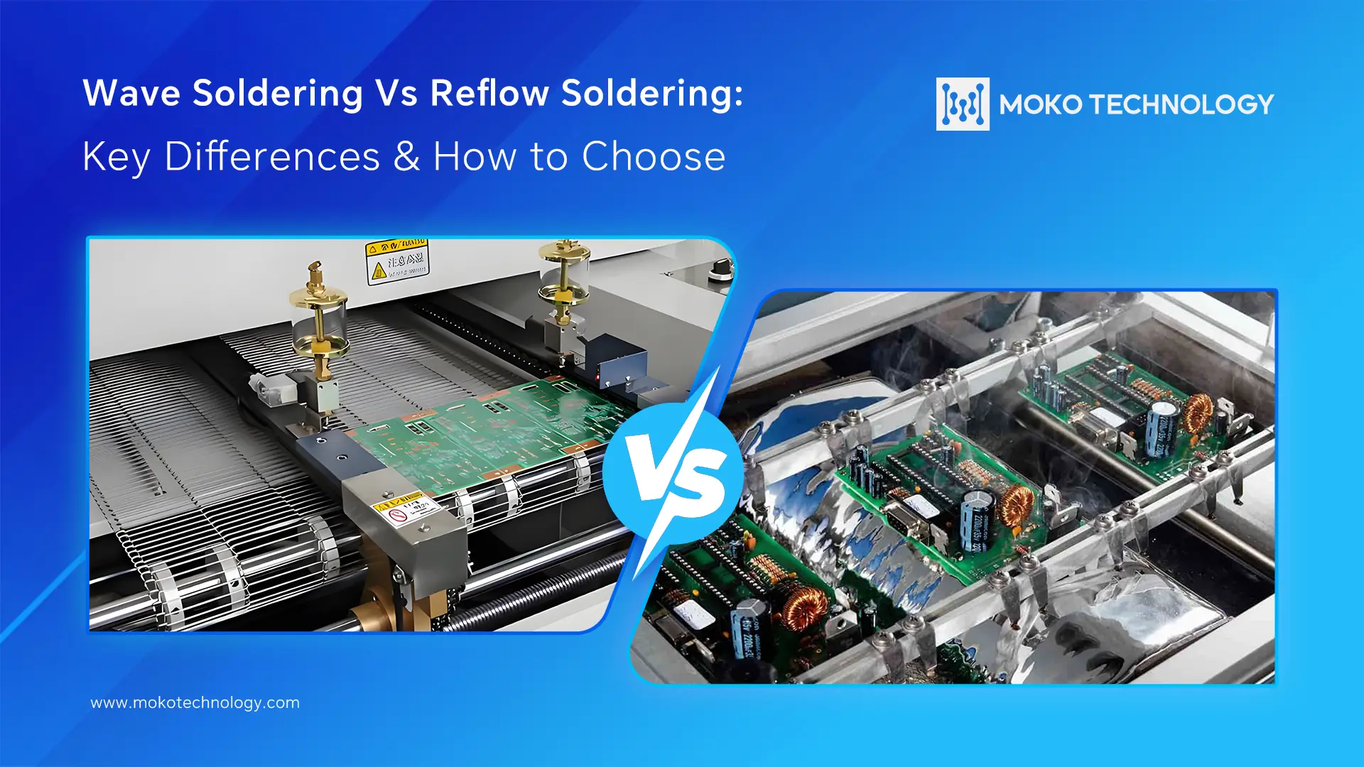
Soldering is an indispensable step in the PCB assembly process, which attaches the components to the circuit boards firmly. Wave soldering and reflow soldering are two popular soldering methods used in the PCB industry. They serve the same purpose but have different applications and operational principles. Understanding their differences and which type of soldering to use in different scenarios is critical. In this blog, we will compare these two methods at different aspects and help you choose the right one for your PCB assembly needs.
What Is Wave Soldering?
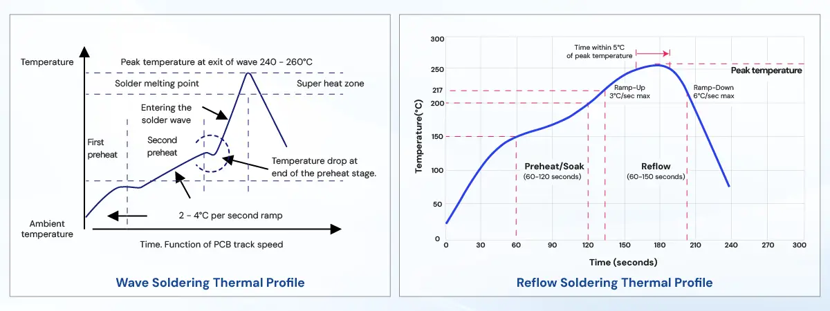
Wave soldering is a method used to attach electronic components onto a circuit board. In the wave soldering process, the board is put into a machine with a pump that creates a “wave” of liquid solder. When the board passes over and comes into contact with the wave, the solder bonds to the parts and board, creating good electrical connections. The method is usually employed for through-hole components and is considered very efficient for mass production. Here is a video that clearly shows the wave soldering process:
What Is Reflow Soldering?
Reflow soldering is a widely used process in the electronics industry for attaching surface-mount components (SMDs) to printed circuit boards. In this process, solder paste is precisely applied to the board at the locations where components will be placed, forming temporary connections. The board is then placed into an oven with a carefully controlled temperature profile, which heats and melts the solder paste so as to create permanent solder joints and stable electrical connections.
Here’s a video that demonstrates the reflow soldering process in action:
Key Differences between Wave Soldering and Reflow Soldering
In this section, we compare wave and reflow soldering across three key aspects: processes, suitable components, and temperature ranges.
- Working Principles and Processes
Wave soldering: Using the molten solder to from wave, and when PCB pass over it, component leads or pads make direct contact with the solder to form mechanical and electrical connections.
Reflow soldering: Solder paste is pre-applied to the pads, then melted by hot air so as to bond component to the circuit board firmly.
On the other hand, wave soldering requires solder flux spraying, while reflow soldering does not, because the solder paste already contains flux. The figures below illustrate each step of the soldering process for both wave and reflow methods:


- Components Compatibility
Wave soldering is primarily used for through-hole components, especially those with large size, robust pins, and higher requirements for structural strength, such as connectors, power transformers, high-capacitance capacitors, power inductors, and power modules.
Reflow soldering is more suitable for SMT components that have small sizes and high-density pins, including the 0402, 0603, and 0805 series of chip resistors and capacitors, packages like QFP, QFN, and BGA, etc. - Temperature Range
Wave soldering and reflow soldering operate at different temperature range. Generally, reflow soldering peaks at 210–250°C in the reflow zone, while wave soldering reaches a higher peak temperature of 260–265 °C. Therefore, when soldering mixed boards that requires to use both reflow soldering and wave soldering techniques, reflow soldering should be performed before wave soldering to avoid re-melting previously formed joints.


Wave Soldering vs. Reflow Soldering: Quick Comparison Table
| Aspect | Wave Soldering | Reflow Soldering |
| Component Type | Mainly through-hole (THT) components | Surface-mount (SMT) components |
| Heating Method | Molten solder wave contacts PCB underside | Controlled heating curve inside reflow oven |
| Mechanical Strength | High; joints suitable for components under mechanical stress | Moderate; joints less robust than wave soldering, sensitive to vibration/stress |
| Precision | Lower; suitable for larger leads and less dense boards | Higher; ideal for fine-pitch SMT and high-density layouts |
| Throughput | Very efficient for large THT batches and mass production | High for SMT boards in automated lines |
| Double-Sided Use | Limited (mainly single-sided) | Widely used; ideal for double-sided SMT boards |
| Ideal Applications | Power boards, connectors, simple assemblies, robust components | High-density consumer electronics, IoT devices, telecom equipment, fine-pitch boards |
Wave Soldering Vs. Reflow Soldering: How to Choose?
Wave soldering and reflow soldering are both effective soldering techniques during the PCB assembly process. But how do you choose the right one for your PCB projects?
First, consider the components types that your PCB projects need. If the PCB primarily uses surface mount devices, then reflow soldering would be your go-to choice. However, if you mainly have through-hole parts, or components that need to handle strong mechanical stress, then you should choose wave soldering.
Additionally, consider other factors such as the production volumes, equipment investment costs, and precision requirements. Reflow soldering excels in automated, high-throughput SMT production, while wave soldering remains more efficient and cost-effective for THT-heavy boards.
In real-world production, many projects require both soldering techniques. Assemble SMT components first, and then use wave soldering or selective soldering to assemble the remaining through-hole components.
To sum up, there is no so-called best soldering method, only one that best fits your PCB design and production needs. Before making the decision, considering all these factors is a must.
Need Expert PCB Soldering Services?
At MOKO Technology, we specialize in both wave soldering and reflow soldering for PCB assembly. Our advanced manufacturing facility is equipped to handle:
– High-volume production with both soldering methods
– Mixed technology assemblies (SMT + THT)
– Strict quality control and IPC standards compliance
– Flexible production scheduling for prototypes to mass production
Whether you need selective wave soldering for through-hole components or precise reflow soldering for fine-pitch SMT devices, our experienced team can deliver reliable results for your project. Contact us today to discuss your PCB assembly needs.
FAQs about Wave Soldering and Reflow Soldering
Q1: What is the main difference between wave soldering and reflow soldering?
Reflow soldering melts solder paste in an oven and is typically used for surface-mount technology, while wave soldering connects parts using a wave of molten solder and is commonly used for through-hole components.
Q2: What are the disadvantages of wave soldering?
Wave soldering is not suitable for all PCB components, as some components may not be able to withstand the high temperature of the solder wave. In addition, it’s hard to control the solder wave precisely, which could cause inconsistent solder quality, such as solder bridges, and may damage sensitive components.
Q3: Can a PCB be assembled using both wave and reflow soldering?
Sure. In mixed-technology PCB designed, it’s common to use both wave and reflow soldering techniques to assemble components.
Q4: Wave Soldering Vs Selective Soldering: What’s the difference?
The key difference is the area of the PCB being soldered. Wave soldering can solder all exposed joints at once by passing the PCB over a continuous solder wave. On the other hand, selective soldering targets only specific through-hole components by using a solder nozzle.