What Is PCBA Manufacturing?
PCBA manufacturing, short for printed circuit board assembly manufacturing, encompasses the intricate process of meticulously placing electronic components onto a printed circuit board (PCB) to culminate in a fully operational printed circuit assembly. Successful execution of the PCBA process necessitates adept management of component supply chains, efficient operation of PCBA production lines, rigorous quality control measures, and comprehensive testing procedures.
The Difference between PCBA and PCB
Before we explain the PCB assembly process, let’s first figure out these two common terms: PCBA and PCB. A PCB acts as the foundation for an electronic device. It’s a bare board made of fiberglass or other material that provides the wiring between components. On its own, a PCB doesn’t actually do anything. It’s like an empty canvas waiting to come alive. A PCBA is what you get when all the necessary components are soldered onto the PCB. This transforms that blank slate into a fully functional circuit board ready for action.
PCBA Manufacturing Process
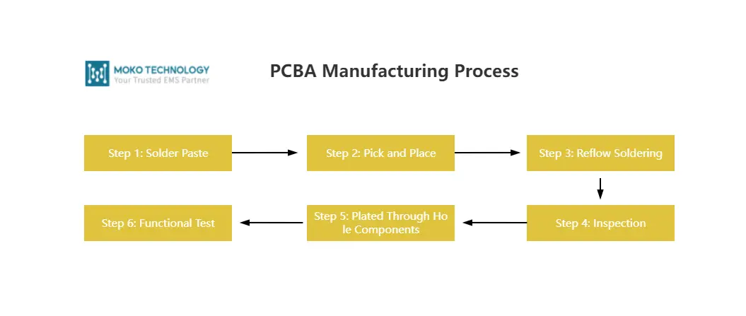
Step 1: Solder Paste
In the first step, a solder paste is put on certain areas of the board where electronic components need to be mounted. The solder paste is made up of various tiny balls of metals, mainly composed of tin accounting for about 96.5%, and other metals including silver and copper. Moreover, the solder paste needs to be mixed with flux so it can melt and stick to the board. To apply solder paste in the precise areas and right amounts, PCBA manufacturers usually use mechanical fixtures to hold the circuit boards and solder stencil. Then use the applicator to apply the right amount of solder paste to the desired area, and when the stencil is removed, the solder paste is in the right place.
Step 2: Pick and Place
The board needs to go through a pick and place process after the solder paste is properly added to the board. Pick up surface mount components from a reel and place them on the intended areas of the board. And the solder paste has enough adhesive strength to hold these components in place. This process can be performed manually or automatically, with most manufacturers currently preferring the latter, as the entire process is performed by a machine, improving both precision and production efficiency. What’s more, automatic pick and place ensure the consistency of PCBA from batch to batch.
Step 3: Reflow Soldering
After placing the surface mount components into the board, PCBA manufacturers conduct reflow soldering to solidify the solder paste, which connects the components with the board firmly. So how does it work? First, the board would be transferred to a conveyor belt that would pass through a large reflow oven. There are a number of heaters in the oven, they heat boards at a temperature of about 250 Celsius until the solder turns into the solder paste. Then, the board would be passed through a series of coolers that can cool down the melted solder paste to create a permanent solder joint so surface mount components can be assembled on the board tightly.
Step 4: Inspection
It has the possibility for circuit boards to have problems like poor connection quality or short circuit after reflow soldering, hence, in this step, manufacturers apply several methods to inspect the PCBA and test the functionality of the board. Below are listed two methods of PCBA testing:
Optical Inspection: Compared to manual inspection, automatic optical inspection is more suitable for inspecting large quantities of PCBA orders, which can find defects and errors in the board with high accuracy and fast speed. During the optical inspection process, an automatic optical machine plays an important role that is equipped with high-powered cameras that can inspect the connection from different angles. In addition, the machine can inspect the quality of connections by analyzing the different light intensities that are reflected from solder connections.
X-Ray Inspection: When it comes to complex and layered circuit boards, X-ray inspection is a perfect choice that uses x-rays to inspect PCBA. By using x-rays, we can see through the layers and find out all errors on the board even problems in the lower layer.
These two inspections are conducted before the final functional test that aims to confirm the board is fully functional.
Step 5: Plated Through Hole Components
Different types of PCBA require to use different electronic components, apart from surface mount components, PTH(Plated Through Hole) components are also widely used. During PTH assembly, holes are drilled into the board so that components on the board can pass signals from one side to the other side of the circuit board. And there are two types of PTH soldering processes:
Manual Soldering: During this process, all components are manually inserted into the board. This is how it works, one person is responsible for inserting one type of component in the desired area, then the board will be transferred to another workstation, another person inserts another type of component, and there will be many stations to do different component insertion tasks until each hole is filled with the correct component.
Wave Soldering: It is another popular soldering process for through-hole printed circuit assemblies. When the PTH components are placed on the board, the board would be transferred by a conveyer that passes across a pumped wave or waterfall of solder. The solder smears the exposed metallic areas of the board to create good mechanical and electrical connections.
Step 6: Functional Test
The last step in PCBA manufacturing is to do final inspection of all PCBAs, that is, functional testing. During this test, PCBA would be tested under the same circumstances in which the circuit will operate. The simulated signals and power signals would run through the PCBA to test the electrical features of the board. If the fluctuations of these features are beyond the allowable range, then the board failed the test.
MOKO Technology Is Your Go-to PCBA Manufacturer
PCB assembly process can be complex for high-density boards with thousands of components, so finding a professional PCB assembly company is of vital importance. MOKO Technology has rich experience in providing PCBA contract manufacturing services. All of our products follow the IPC-A-610 standards. Moreover, we provide a one-stop PCB assembly service, from design to assembly and testing. Contact us now to start your PCBA project!