Printed circuit boards are the key to the operation of electronics, therefore, it’s imperative to ensure their quality before officially putting them into use. There are many PCB testing methods to check the quality of PCBs, and one powerful way that has revolutionized the inspection process is PCB X-ray Inspection. This non-destructive method enables manufacturers to identify hidden defects and ensure the reliability and performance of electronic devices. In this blog, we will delve into the world of PCB X-ray Inspection, exploring its types, working principles, the defects it can detect, and its benefits.
What Is PCB X-Ray Inspection?
X-ray technology has found widespread application in various industries, including aerospace and medical fields, for detecting manufacturing errors. In the PCB industry, X-ray inspection has gained immense popularity as a reliable method for analyzing the internal structures of printed circuit boards. Manufacturers leverage this technology to unveil hidden defects without causing any damage to the board itself.
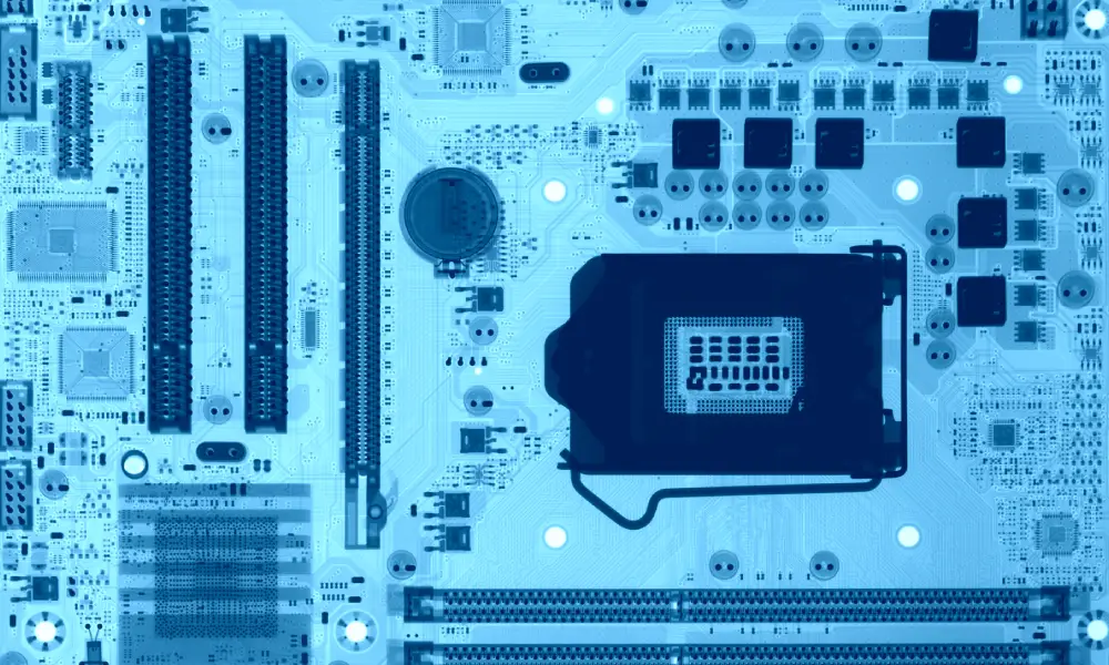
The process involves utilizing X-ray radiation to penetrate the PCB, capturing detailed images of its internal components. The primary goal is to identify defects that may not be visible through conventional visual inspection methods.
Types of PCB X-Ray Inspection
There are two X-ray inspection methods used to check the quality of printed circuit boards, they are:
Manual X-ray inspection system
In this inspection system, the manufacturer manually inserts the PCB into the system for analysis. The system generates an image of the board, allowing for a focused examination of specific areas of interest. This image is displayed on the screen, providing valuable information about the metrology and quantitative features of the photo.
One of the key advantages of a manual X-ray inspection system is its ability to turn dimensional measurements into quantitative information. In spite of that, it is crucial to note that not all manual systems have automatic analysis capabilities. In such cases, the operator must rely on their expertise and observation skills to evaluate the board under inspection. This requires the inspector to effectively distinguish between good and faulty connections by comparing the observed board with reference boards.
Automated X-ray inspection
Automated PCB X-ray inspection systems are particularly well-suited for high-volume PCB production. Compared to manual systems, automated inspection offers greater efficiency and meets the demands of large-scale manufacturing. These systems are designed to seamlessly handle circuit boards, whether they are received from robotic handlers or cartridges.
In automated X-ray inspection, a computer oversees the image-acquiring and board-loading processes. The computer’s level of sophistication enables it to make pass-or-fail decisions based on quality criteria predetermined by the system. Additionally, it can transmit test data for further statistical analysis, providing valuable insights for process improvement.
Due to the limitations of capturing the entire PCB in a single X-ray photo, the computer-driven system precisely positions the PCB and automatically acquires images from different angles. Subsequently, the computer analyzes the gathered image information to determine whether any rework is necessary. It’s important to note that training the system is crucial as it relies on the computer to carry out the inspection steps effectively.
How X-Ray Inspection Works?
X-ray inspection operates through three fundamental components that make up the inspection device:
X-ray Tube: This component generates X-ray photons, which are essential for the inspection process.
Operation Platform: The operation platform serves the purpose of maneuvering the sample being inspected. It allows the sample to be moved in various directions and angles, ensuring comprehensive inspection.
Detector: Positioned on the opposite side of the sample, the detector plays a crucial role in capturing and collecting X-ray photons. It then converts them into a visual image for analysis.
The X-ray imaging test relies on the interaction of X-ray photons with the target material placed on the operation platform. As the X-ray photons go through the material, they undergo differential absorption based on the material’s physical properties, such as density, atomic weight, and thickness.
The principle of differential absorption states that heavier objects absorb more X-rays, resulting in the development of a clearer image. Conversely, lighter objects tend to be more transparent to X-rays. The distinctive attributes of each object result in varying quantities of X-ray photons being gathered on the opposing side of the target material, ultimately forming the final image. Given that PCB components typically consist of heavier elements, their internal parts are easier to visualize and analyze in an X-ray image. This characteristic enables X-ray inspection to effectively detect and identify defects or irregularities within the printed circuit board.
Common Defects Found through X-Ray Inspection
X-ray systems are capable of detecting numerous defects in PCBs that may be challenging to identify through optical or electrical tests alone. This is attributed to the high penetrating power of X-rays. Let’s explore some common faults that can be detected through X-ray PCB inspection:
- Older Joint Issues: X-ray inspection can reveal poor solder quality, insufficient or excessive solder, and the presence of voids or air pockets within solder joints.
- Shorts and Opens: X-ray analysis is effective in identifying short circuits caused by solder bridging or conductive debris. It can also detect open circuits resulting from broken traces or missing solder connections.
- Component Misalignment: X-ray inspection helps uncover misalignment or incorrect placement of components on the PCB, ensuring precise positioning and alignment.
- Internal Delamination: X-rays can penetrate the layers of a PCB and detect internal delamination, which refers to the separation or detachment of layers within the board.
- Component Integrity: X-ray inspection can verify the integrity of components by revealing internal cracks, voids, or other physical defects that may impact their performance and reliability.
- Wire Bond Quality: X-ray systems are capable of inspecting wire bonds in semiconductor devices, ensuring their proper placement, alignment, and bonding quality.
Benefits of X-Ray Inspections
- Enhanced Defect Detection
X-ray inspection can unveil hidden defects that may not be visible to the naked eye. By utilizing X-ray radiation, manufacturers can ensure higher quality standards and minimize the risk of product failures.
- Non-Destructive Testing
X-ray inspection enables manufacturers to thoroughly inspect the boards without compromising their functionality. It not only saves time and resources but also ensures that the PCBs maintain their structural integrity throughout the inspection process.
- Increased Efficiency and Accuracy
It enhances the speed and precision of the inspection process, reducing the need for manual inspection and minimizing the potential for human error. By automating the inspection process, manufacturers can achieve higher throughput rates, allowing for a greater number of PCBs to be inspected within a shorter timeframe.
- Solder Joint Evaluation
X-ray inspections allow detailed evaluation of solder joints, especially in complex or miniaturized assemblies. By analyzing the solder joint quality, including the fillet formation and the presence of voids or defects, potential weaknesses can be identified, preventing solder-related failures and ensuring robust connections.
- Identify Pin-hole Fills
Insufficient pin-hole fill for through-hole connectors is a frequent issue encountered in circuit boards. X-ray machines offer a solution to detect such errors and provide a quantitative assessment of the missing fill using coordinate measurements.
Conclusion
PCB X-ray inspection has emerged as a vital tool for defect detection, offering an in-depth analysis of PCB structures and uncovering hidden defects. By leveraging the power of X-ray technology, manufacturers can enhance quality control, minimize production errors, and deliver electronic devices that meet the highest standards. Embracing PCB X-ray Inspection is a step toward achieving excellence in electronics manufacturing. MOKO Technology implements 100% PCB inspection and ensures the best quality by implementing various inspection methods including X-ray inspection, flying probe test, functional test, etc. Get in touch with us now to kick-start your project!