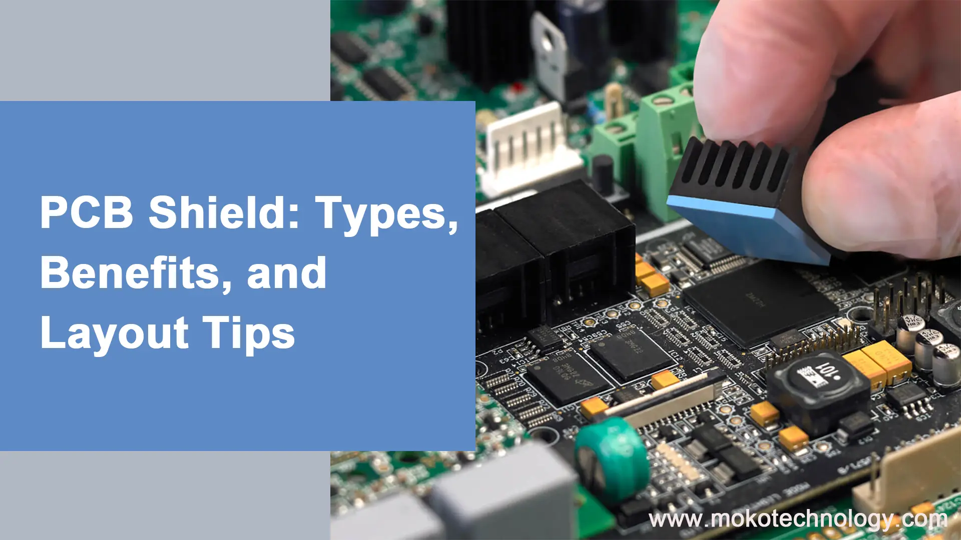
PCB Design

How to Design Effective Bluetooth Circuit Boards

How to Design Effective Bluetooth Circuit Boards?

Bluetooth is everywhere these days! You can find it in smartphones, headphones, speakers – pretty much any gadget that connects wirelessly likely uses Bluetooth. So when building a new electronic product that needs wireless functionality, adding Bluetooth usually makes sense. To make that happen, you typically need a custom-designed Bluetooth circuit board. In this blog

How to Design Effective Bluetooth Circuit Boards? Read More »

PCB Trace Width: Why It Matters for Your Board Performance

PCB Trace Width: Why It Matters for Your Board Performance

PCB trace width specifically refers to the width of copper traces that carry vital signals and power across the printed circuit board. Determining appropriate trace widths is an important PCB design consideration impacting current density, temperature rise, signal integrity, manufacturability, and more. There is no one-size-fits-all trace width that will work for every unique situation. Instead, finding

PCB Trace Width: Why It Matters for Your Board Performance Read More »

PCB Transmission Line: What Is It? Why Is It Important?

The growing demand for advanced electronics drives innovations in circuit board capabilities and performance. Circuit designers now routinely work with faster signal speeds. High-speed signals, once an occasional challenge, are becoming standard in printed circuit board layouts. Flawless transmission of high-speed signals requires designers to understand best practices for routing traces on boards. Traces can

PCB Transmission Line: What Is It? Why Is It Important? Read More »

Stacked Via VS. Staggered Via: What’s the Difference

Stacked Via VS. Staggered Via: What’s the Difference?

A common question when designing complex printed circuit boards for advanced electronics is whether to use stacked or staggered vias to route connections between layers. Vias act as conductive pathways through the interior layers of multilayer circuit boards. Understanding the key differences between vertically stacking vias atop one another versus horizontally offsetting them enables choosing

Stacked Via VS. Staggered Via: What’s the Difference? Read More »

How to Design a PCB Schematic: A Step-by-Step Guide

PCB Schematic: What Is It? Why Is It Important? A printed circuit board design starts with a PCB schematic diagram. This PCB schematic layout visually depicts the electronic circuit as a graph, using symbols to represent components and lines to show their electrical connections. Typically, the PCB schematic is developed prior to the physical board layout. Once

How to Design a PCB Schematic: A Step-by-Step Guide Read More »

PCB Fiducial Mark Guide

PCB Fiducial Mark: A Comprehensive Guide for Beginners

Fiducial marks, also known as fiducials, are small copper markers printed on PCB that serve as visual reference points during assembly and inspection, allowing automated assembly machines and quality control systems to precisely locate specific features and components.  PCB fiducial mark typically consists of circular pads or other exposed copper shapes surrounded by clearance areas.

PCB Fiducial Mark: A Comprehensive Guide for Beginners Read More »

Scroll to Top