At what frequency do PCB traces start to act as antennas?

Just interested in PCB design. I am wondering whether PCB traces start to act as antennas at some frequency. Anybody knows?

Frequencies where the length of the trace is comparable to 1/10th of the wavelength of the wave in air is a decent rule of thumb I’ve heard.

However, you should still be watching out to avoid accidental antenna problems.

  • Avoid ground loops. Use a single point as ground (usually a plane at the bottom of the PCB), and don’t route the ground of one point through the ground at another point. Ground loops can cause really big signal integrity problems.
  • Where possible, use differential signaling — that is, a pair of wires or traces — to send signals, and receive them with differential amplifiers.

Read More: Telecom Electronics Manufacturing

#PCB Design
Picture of Oliver Smith

Oliver Smith

Oliver is an experienced electronics engineer skilled in PCB design, analog circuits, embedded systems, and prototyping. His deep knowledge spans schematic capture, firmware coding, simulation, layout, testing, and troubleshooting. Oliver excels at taking projects from concept to mass production using his electrical design talents and mechanical aptitude.

What Others Are Asking

Why do some through-hole LEDs have flared leads?

I have worked with many through-hole LEDs over the years. I ordered a bunch for a personal project. I did not notice they have flared leads until I used them. I’ve never encountered these flared leads before. What is their purpose?

Read Detailed Advice From Blog Articles

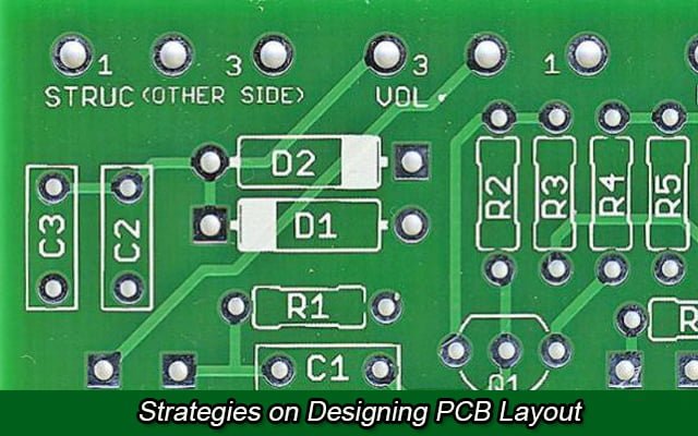
Strategies on Designing PCB Layout
Ryan Chan

Strategies on Designing PCB Layout

Why PCB Layout is Needed We use Printed Circuit Boards (PCB) for connecting electronic components by using conductive tracks. This allows for prototyping electric circuits

Scroll to Top