How can I indicate pin 1 on a SMT package footprint without silkscreen?

Sometimes when I order PCBs from a board house, I omit the bottom silkscreen for budgetary reasons. When I place surface-mount chips on the bottom of the board, I then end up with a footprint that doesn't indicate the chip orientation. How can I clearly indicate pin 1 with the remaining layers in a way that will be clear but not significantly impact the PCB size or cause issues when soldering?

Have a differently shaped solder mask on pin 1.

For surface mount processors, you could have the pin 1 pad be noticeably longer than the others.

Read More: SMT Assembly

#PCB Assembly  #PCB Manufacturing

Picture of Oliver Smith

Oliver Smith

Oliver is an experienced electronics engineer skilled in PCB design, analog circuits, embedded systems, and prototyping. His deep knowledge spans schematic capture, firmware coding, simulation, layout, testing, and troubleshooting. Oliver excels at taking projects from concept to mass production using his electrical design talents and mechanical aptitude.

What Others Are Asking

Do ICs have a shelf life?

What I would like to know is if ICs also have a limited shelf life and if so, do some types suffer more than others?

Read Detailed Advice From Blog Articles

Guide to PCB manufacturing
Will Li

A Detailed Guide to the PCB Manufacturing Process

Introduction PCBs (printed circuit boards) form the foundation of contemporary electronic devices, ranging from handheld devices like mobile phones to advanced spacecraft technologies. They are
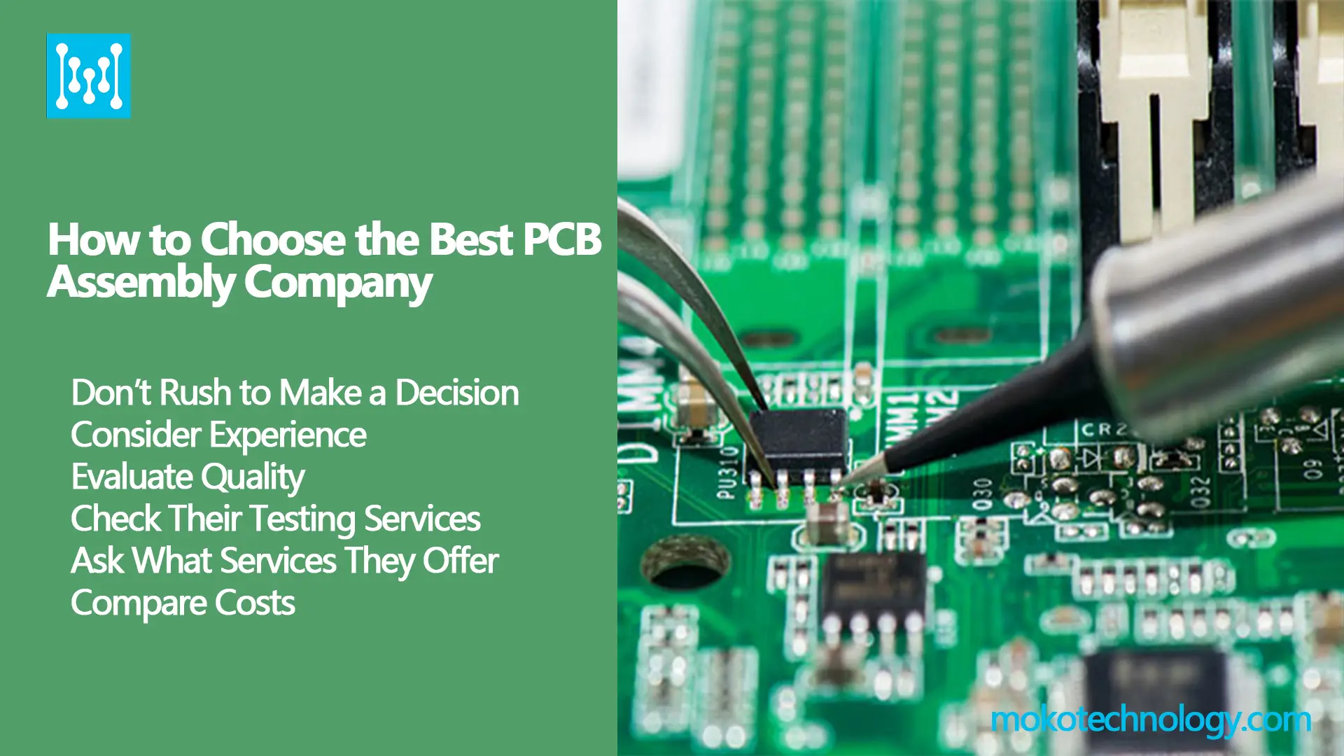
Scroll to Top